Phase changeable memory devices

a memory device and phase change technology, applied in the field of semiconductor memory devices, can solve the problems of large current required, failure to meet the requirements of read operation, and increased area of capacitor electrodes,

Active Publication Date: 2006-10-03
SAMSUNG ELECTRONICS CO LTD
View PDF18 Cites 192 Cited by
  • Summary
  • Abstract
  • Description
  • Claims
  • Application Information

AI Technical Summary

Benefits of technology

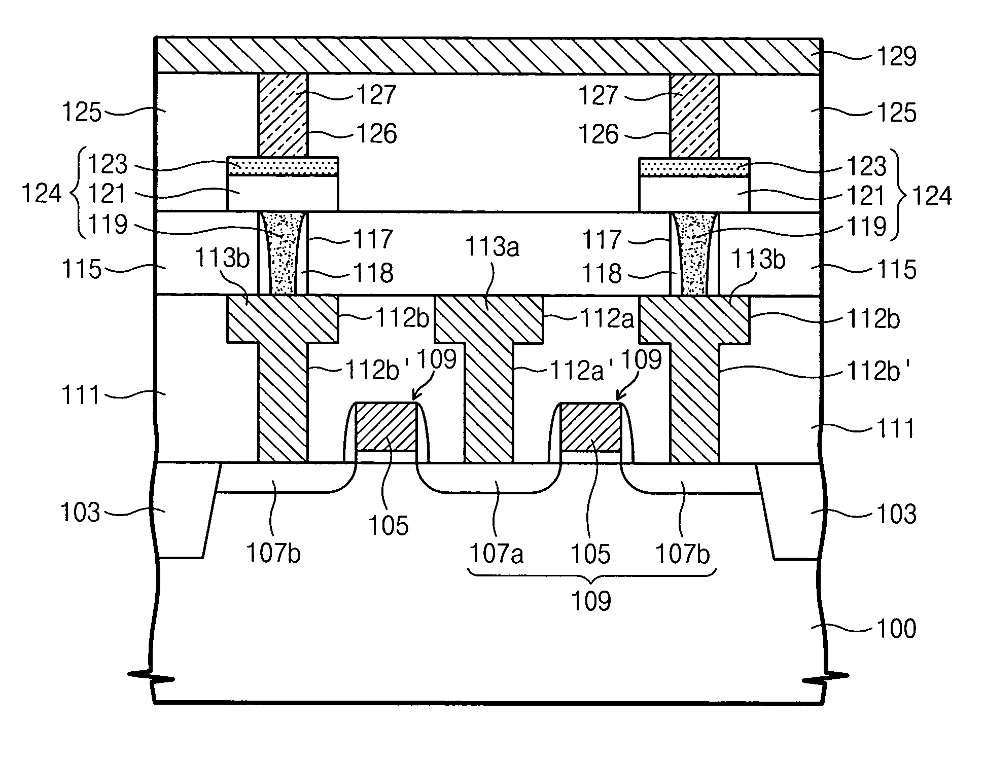
[0019]In additional embodiments of the present invention, the phase-changeable material pattern has a polycrystalline structure having 100 nm grains or smaller. The amount of the nitrogen atoms may be about from 0.25% to about 25% with respect to a total atomic weight of ingredients of the phase-changeable material pattern. The phase-changeable material pattern may be Ge—Sb—Te—N, As—Sb—Te—N, As—Ge—Sb—Te—N, Sn—Sb—Te—N, In—Sn—Sb—Te—N, Ag—In—Sb—Te—N, a 5A group element-Sb—Te—N, a 6A group element-Sb—Te—N, a 5A group element-Sb—Se—N, and/or a 6A group element-Sb—Se—N. The bottom and top electrodes may be a conductive material containing nitrogen, a conductive material containing carbon, titanium, tungsten, molybdenum, tantalum, titanium silicide, tantalum suicide, and/or a combination thereof.
[0020]In still further embodiments of the present invention, a top surface of the top electrode is lower than a top surface of the upper intermetal dielectric layer. A conductive plug penetrates the intermetal dielectric lay...

Problems solved by technology

For instance, increasing the surface area of capacitor electrodes may increase the capacitance but the surface area increase of the capacitor electrode may be an obstacle ...

Method used


Image

  • Phase changeable memory devices
  • Phase changeable memory devices
  • Phase changeable memory devices

Examples


Embodiment Construction

[0035]The present invention will now be described more fully with reference to the accompanying drawings, in which preferred embodiments of the invention are shown. This invention may, however, be embodied in different forms and should not be construed as being limited to the embodiments set forth herein. Rather, these embodiments are provided so that this disclosure will be thorough and complete, and will fully convey the scope of the invention to those skilled in the art. In the drawings, the size or thickness of layers and regions are exaggerated for clarity. Like numbers refer to like elements. As used herein the term “and / or” includes any and all combinations of one or more of the associated listed items.

[0036]It will be understood that although the terms first and second may be used herein to describe various regions, layers, and / or sections, these regions, layers, and / or sections should not be limited by these terms. These terms are only used to distinguish one region, ...


PUM


Abstract

Phase-changeable memory devices and method of fabricating phase-changeable memory devices are provided that include a phase-changeable material pattern of a phase-changeable material that includes nitrogen atoms. First and second electrodes are electrically connected to the phase-changeable material pattern and provide an electrical signal thereto. The phase-changeable material pattern may have a polycrystalline structure.

Description

CLAIM OF PRIORITY[0001]This application claims priority from Korean Patent Application No. 2003-11416, filed on Feb. 24, 2003, in the Korean Intellectual Property Office, the contents of which are incorporated herein by reference in its entirety.FIELD OF THE INVENTION[0002]The present invention relates to semiconductor memory devices and more specifically to phase-changeable memory devices and methods of fabricating the same.BACKGROUND OF THE INVENTION[0003]Semiconductor memory devices are typically categorized into volatile memory devices and non-volatile memory devices depending on whether data can be conserved or not when power is removed from the device. Volatile memory devices include D-RAM devices and S-RAM devices and non-volatile memory devices include flash memory devices. These memory devices, typically, indicate logic “0” or “1” according to the presence of stored charge.[0004]D-RAM (i.e. a volatile memory device) typically requires periodic refresh operations and a high ...

Claims


Application Information

Patent Timeline
IPC IPC(8): H01L27/108H01L29/02H01L29/76H01L29/94H01L31/119H01L27/115G11C16/02H01L27/105H01L27/24H01L45/00
CPCG11C13/0004H01L27/2436H01L45/06H01L45/1233H01L45/143H01L45/144H01L45/1625H01L45/1675G11C2213/79H01L2924/0002Y10S257/904H01L2924/00H10B63/30H10N70/231H10N70/8825H10N70/026H10N70/826H10N70/8828H10N70/063
Inventor HIDEKI, HORIIPARK, JEONG-HEE
Owner SAMSUNG ELECTRONICS CO LTD
Why Eureka
Try Eureka