Integrated circuit and fabrication process

a technology of integrated circuits and fabrication processes, applied in the field of analog devices, can solve the problems of low capacitor capacitance, inability to differentiate several charge levels of capacitors, and inability to stabilize capacitors,

Inactive Publication Date: 2006-10-03
STMICROELECTRONICS SRL
View PDF5 Cites 5 Cited by
  • Summary
  • Abstract
  • Description
  • Claims
  • Application Information

AI Technical Summary

Benefits of technology

[0023]The invention also makes it pos...

Problems solved by technology

In addition, for the sake of the memory cell density, the capacitance of the capacitor is low, and it is then impossible to differentiate several charge levels of...

Method used


Image

  • Integrated circuit and fabrication process
  • Integrated circuit and fabrication process
  • Integrated circuit and fabrication process

Examples


Embodiment Construction

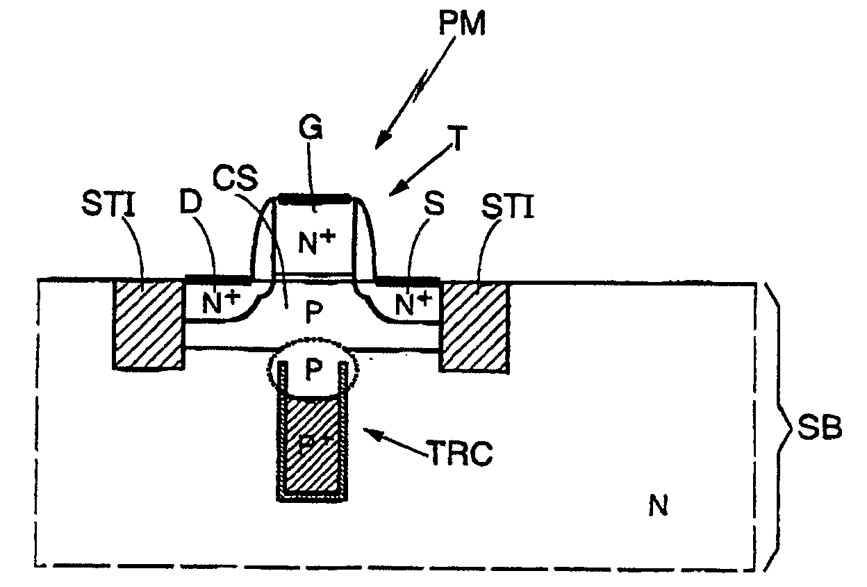
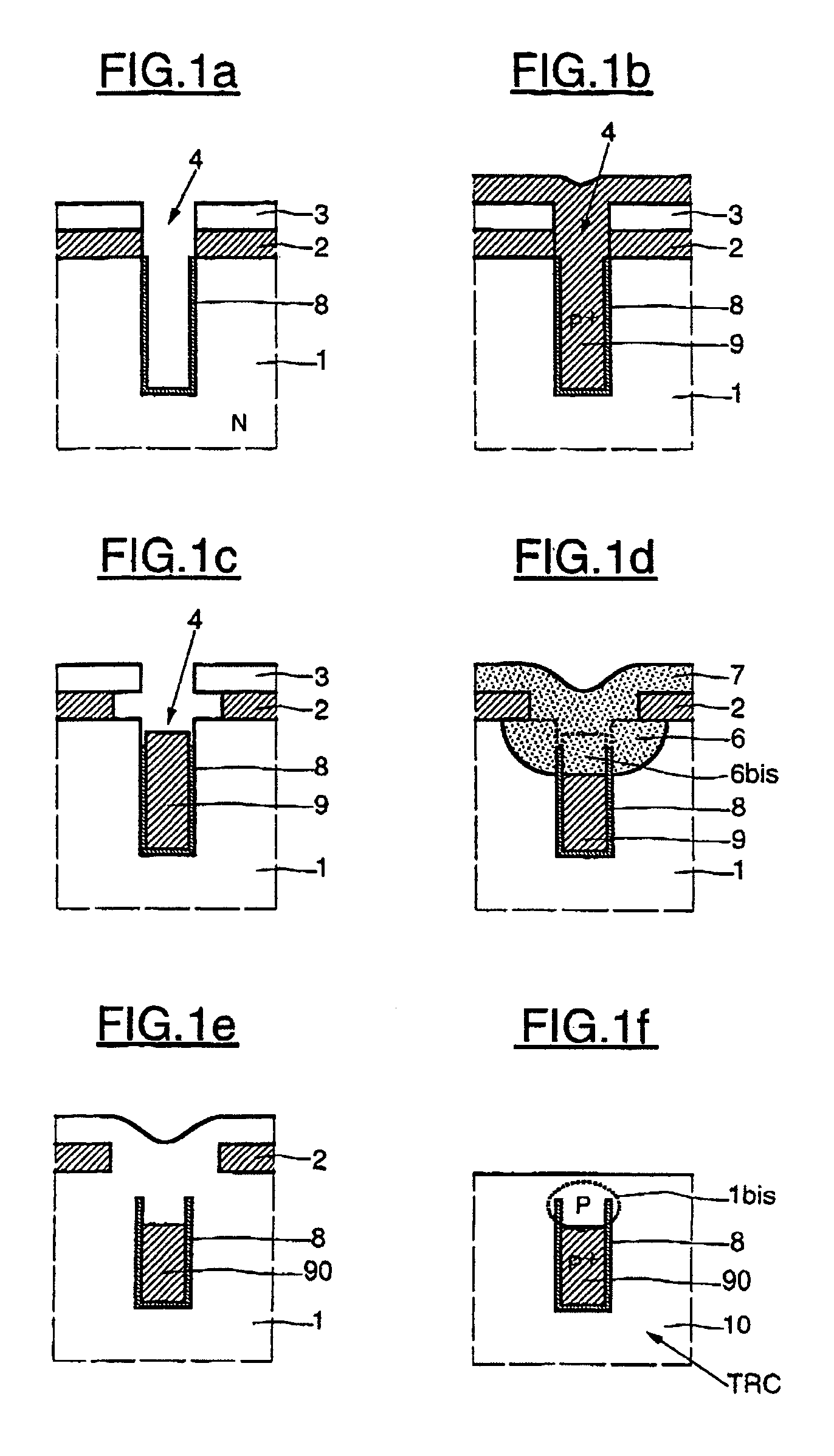
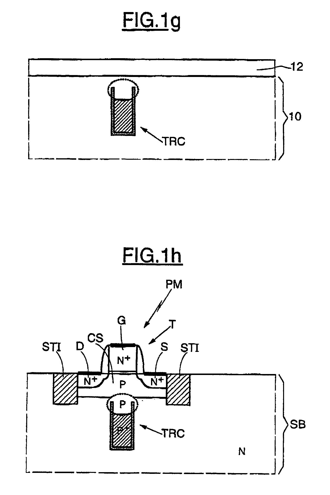
[0045]The starting substrate of the process of the invention, or the initial substrate, is illustrated in FIG. 1a and in this case comprises an elementary trench. In this case, the initial substrate 1 is n-doped. The elementary trench may be made, according to one implementation of the process of the invention, by firstly depositing a layer of silicon oxide 2 on the initial single-crystal silicon substrate 1. The thickness of this layer 2 may vary between 0.01 micron and 1 micron, and is preferably about 2000 Å.

[0046]Next, a layer of silicon nitride 3 is deposited on the oxide 2. The thickness of this layer 3 may also vary between 0.01 micron and 1 micron, and is also preferably about 2000 Å.

[0047]Next, first of all the nitride 3 and the oxide 2, then finally the single-crystal silicon of the substrate 1 are etched in a conventional manner using a photolithography operation, in order to form the elementary trench 4.

[0048]The elementary trench 4 has a depth of about 6 μm and a width,...


PUM


Abstract

An integrated circuit has at least one semiconductor device for storing charge that includes at least one elementary active component and at least one elementary storage capacitor. The device includes a substrate having a lower region containing at least one buried capacitive elementary trench forming the elementary storage capacitor, and an elementary well located above the lower region of the substrate and isolated laterally by a lateral electrical isolation region. The elementary active component is located in the elementary well or in and on the elementary well. The capacitive elementary trench is located under the elementary active component and is in electrical contact with the elementary well. In one preferred embodiment, the lateral electrical isolation region is formed by a trench filled with a dielectric material and has a greater depth than that of the elementary well. Also provided is a method for fabricating an integrated circuit that includes a semiconductor device for storing charge.

Description

[0001]This application is a 371 of PCT / FR02 / 00054 filed Jan. 9, 2002.FIELD OF THE INVENTION[0002]The invention relates to integrated circuits and more particularly to analog devices for storing charge, in particular analog memory cells or light sensors.BACKGROUND OF THE INVENTION[0003]Electronic memories usually operate with two logic levels 1 and 0. For dynamic random access memory (DRAM memory), these levels correspond to the charged or uncharged state of a capacitor. Reading the memory cell destroys the state of this memory cell since the charges stored in the capacitor are used as a read signal. In addition, for the sake of the memory cell density, the capacitance of the capacitor is low, and it is then impossible to differentiate several charge levels of the capacitor. Moreover, because of the various leakage currents associated with the control devices, the charge on the capacitor decreases and is not stable with time.[0004]A memory cell of the DRAM type must be as small as po...

Claims


Application Information

Patent Timeline
IPC IPC(8): H01L27/108H01L27/10H01L29/68H01L21/8242
CPCH01L27/10832H01L27/10861H01L27/10873H01L27/14683H01L29/808H10B12/373H10B12/038H10B12/05
Inventor MENUT, OLIVIERGRIS, YVON
Owner STMICROELECTRONICS SRL
Why Eureka
Try Eureka