Methods for optimizing package and silicon co-design of integrated circuit

a technology of integrated circuits and optimization methods, applied in the field of integrated circuits, can solve the problems of high detailed studies and extensive development schedules, no fixed or exact sequence of effort in silicon design, package design, board design, electrical modeling, etc., and achieve the effect of efficient development cycles for both silicon and package components

Active Publication Date: 2006-10-03
BELL SEMICON LLC
View PDF7 Cites 15 Cited by
  • Summary
  • Abstract
  • Description
  • Claims
  • Application Information

AI Technical Summary

Benefits of technology

[0008]It is an additional object of the present invention to provide a design method that is integrated and affords efficient development cycles for both silicon and package components.
[0009]It is another object of the present invention to provide a design method that avoids iteration between package design and silicon design since iteration may result in major reworks in both areas.
[0010]It is a further object of the present invention to provide a design method that addresses complex signal integrity constraints imposed by high-speed IO interfaces.
[0012]It is yet still a further object of the present invention to provide a design method that is scalable for all package and silicon co-design applications across all technologies, wirebond, and flipchip package types.

Problems solved by technology

This level of customization may result in highly detailed studies and extensive development schedules during package and silicon co-design.
It is noteworthy that there is no fixed or exact sequencing of effort in the areas of Silicon Design, Package Design, Board Design, or Electrical Modeling.
Design specific constraints often dictate the number of times and at which points each area is revisited.
However, the conventional approaches have the following disadvantages.
First, in practice, the conventional work flow may be highly iterative.
Undesirable impacts of these changes may only be exposed during electrical modeling, which may force the silicon designer to move other IO circuits on the die, or reconsider the necessity of the specific SERDES placement location.
Moreover, the conventional approaches may result in long Silicon and Package co-design development cycles since each area need be re-evaluated multiple times, and in some cases, completely restarted.
Furthermore, the conventional work flow has no closed loop controllability and as a result, it becomes difficult to predict cycle times for a given Silicon and Package co-design exercise.
In addition, supporting such a work flow requires extensive resourcing to service the many and often fine grained iterations between Silicon, Package, Board Designs and Electrical Modeling.
The manpower resourcing of the conventional approaches is therefore very costly.
This often requires costly tool investment and development.

Method used


Image

  • Methods for optimizing package and silicon co-design of integrated circuit
  • Methods for optimizing package and silicon co-design of integrated circuit
  • Methods for optimizing package and silicon co-design of integrated circuit

Examples


Embodiment Construction

[0024]Reference will now be made in detail to the presently preferred embodiments of the invention, examples of which are illustrated in the accompanying drawings.

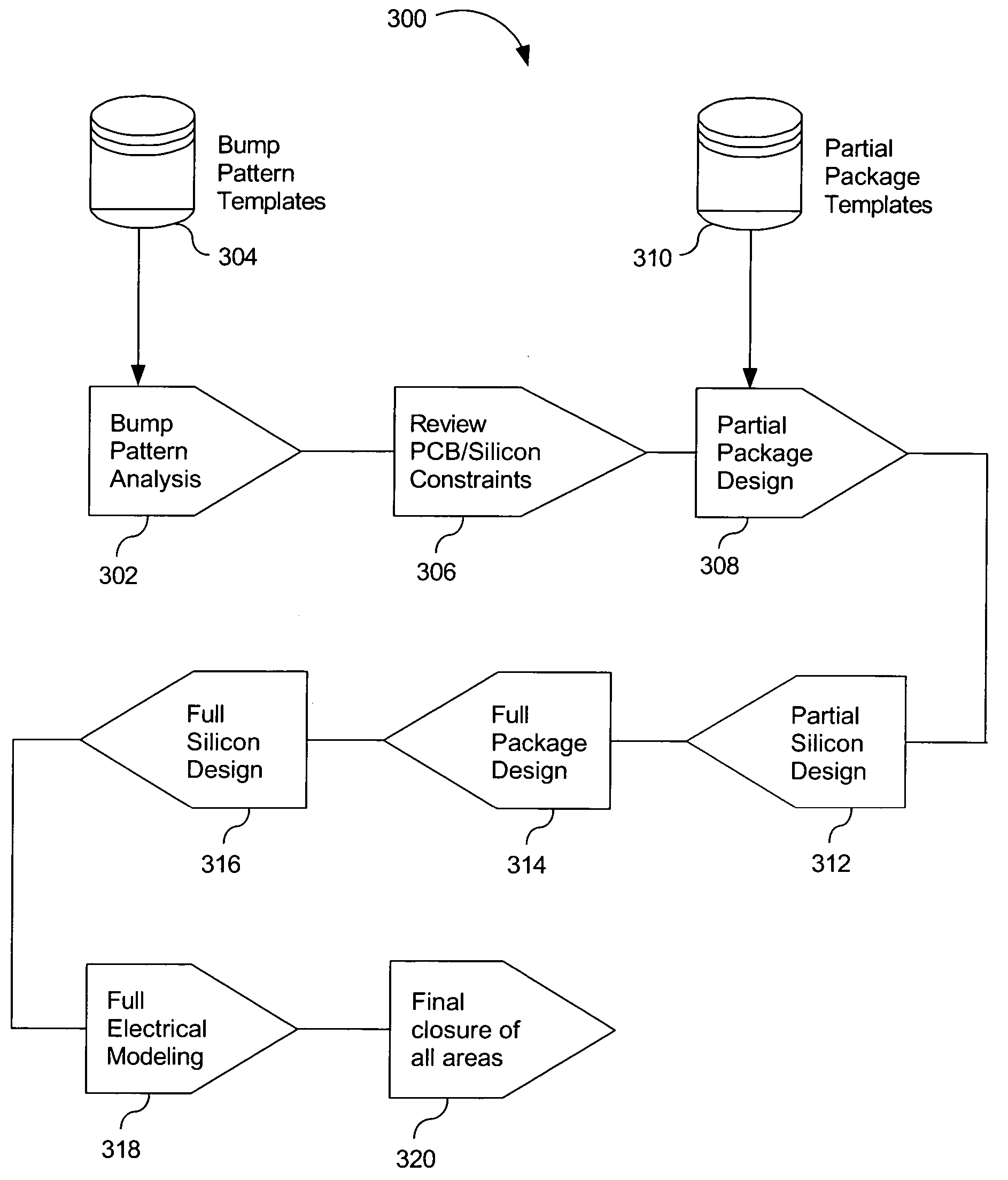
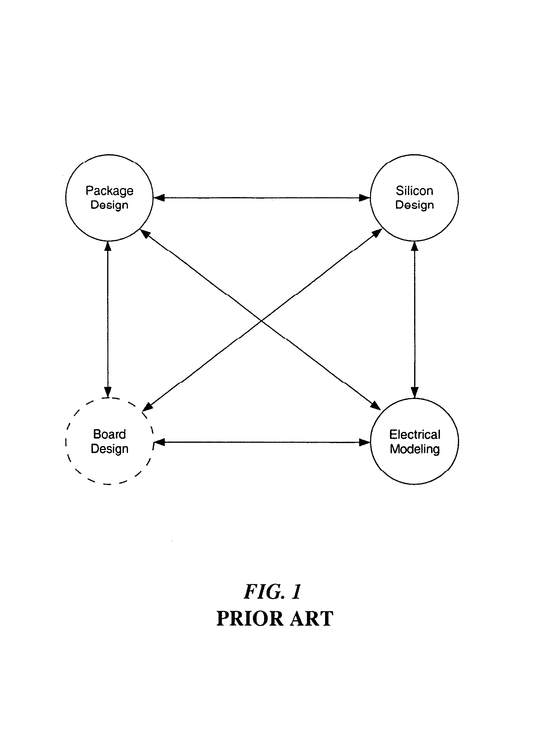
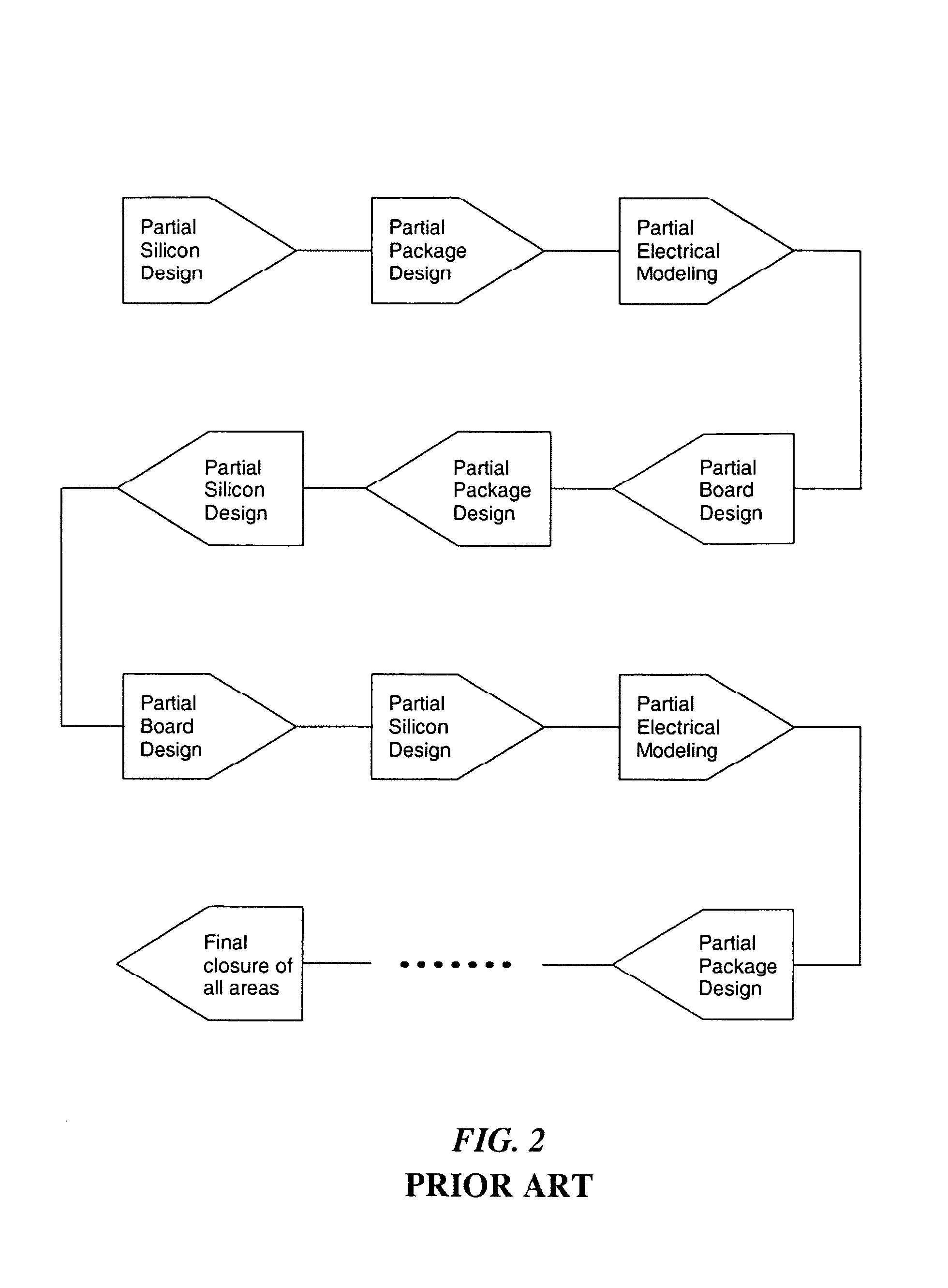
[0025]The present invention provides new methods for silicon and package co-design. Traditional approaches introduce highly iterative steps between silicon, package, and board design, and electrical modeling. These approaches prove to be costly from several aspects including automation and engineering effort. The present approach may eliminate iteration by creating bump and package templates, which can be quickly assembled for a specific design scenario by manual or automation methods. These templates are pre-designed and characterized building blocks for specific portions of a die or IP (Intellectual Property) interface. The present approach may remove the need for iteration and reduce cycle times.

[0026]According to the present invention, two template libraries are present. One library includes bump pattern templates, and...


PUM


Abstract

The present invention is directed to methods for optimizing package and silicon co-design of an integrated circuit. A composite bump pattern for an integrated circuit is created based on a first library including at least one bump pattern template. PCB and Die constraints of the integrated circuit are then reviewed. A partial package design for the integrated circuit is generated based on a second library including at least one partial package template. A partial silicon design for said integrated circuit is started. A full package design for the integrated circuit is then completed. A full silicon design for the integrated circuit is completed.

Description

FIELD OF THE INVENTION[0001]This invention relates generally to integrated circuits, and particularly to methods for optimizing package and silicon co-design of an integrated circuit.BACKGROUND OF THE INVENTION[0002]Modern semiconductors are assembled in either wirebonded or flipchip packages. In either case, the package provides the interconnect between the fine geometries of the silicon design and wider pitches at the circuit board level. The package also serves as environmental protection for the silicon die. With increasing IO (Input / Output) densities and total IO counts, faster signaling speeds, and sharper IO slew rates, the package interconnect has become an integral part of both the silicon and board level design considerations. Specifically, it has forced the need for packages which are highly tuned and customized to a particular silicon design and board application. This level of customization may result in highly detailed studies and extensive development schedules during...

Claims


Application Information

Patent Timeline
Patent Type & Authority Patents(United States)
IPC IPC(8): G06F17/50H01L21/44H01L21/48H01L21/50H01L23/488
CPCG06F17/5068G06F30/39
Inventor ALI, ANWARMIHELCIC, STANMONTHIE, JAMES G.
Owner BELL SEMICON LLC
Why Eureka
Try Eureka