
Embedded heat spreader ball grid array

a technology of heat spreader and ball grid array, which is applied in the direction of semiconductor devices, semiconductor/solid-state device details, electrical apparatus, etc., can solve the problem of low thermal resistance at the interface between die and heat spreader, and achieve the effect of maximizing the available area for package marking, sacrificing thermal performance, and low thermal resistan

Inactive Publication Date: 2006-10-24
AMKOR TECH SINGAPORE HLDG PTE LTD
View PDF45 Cites 105 Cited by
  • Summary
  • Abstract
  • Description
  • Claims
  • Application Information

AI Technical Summary

Benefits of technology

[0008]Attaching the heat spreader directly to the die surface results in a very low thermal resistance at interface between the die and heat spreader. The design of the heat spreader then allows heat to be spread laterally in the package and dissipated through the top and bottom surfaces of the package. Completely embedding the heat spreader in the encapsulant with only a thin layer of material over the upper portions of the heat spreader and between the heat spreader and the substrate accommodates mechanical tolerance stackup of die thickness, bondline thickness, and heat spreader thickness without sacrificing thermal performance. This also maximizes the available area for package marking and improves the cosmetic appearance of the package.

Problems solved by technology

Attaching the heat spreader directly to the die surface results in a very low thermal resistance at interface between the die and heat spreader.

Method used


Image

  • Embedded heat spreader ball grid array
  • Embedded heat spreader ball grid array
  • Embedded heat spreader ball grid array

Examples


Embodiment Construction

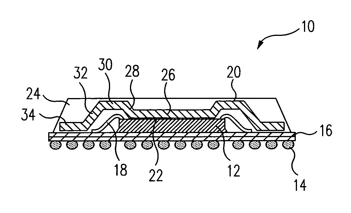
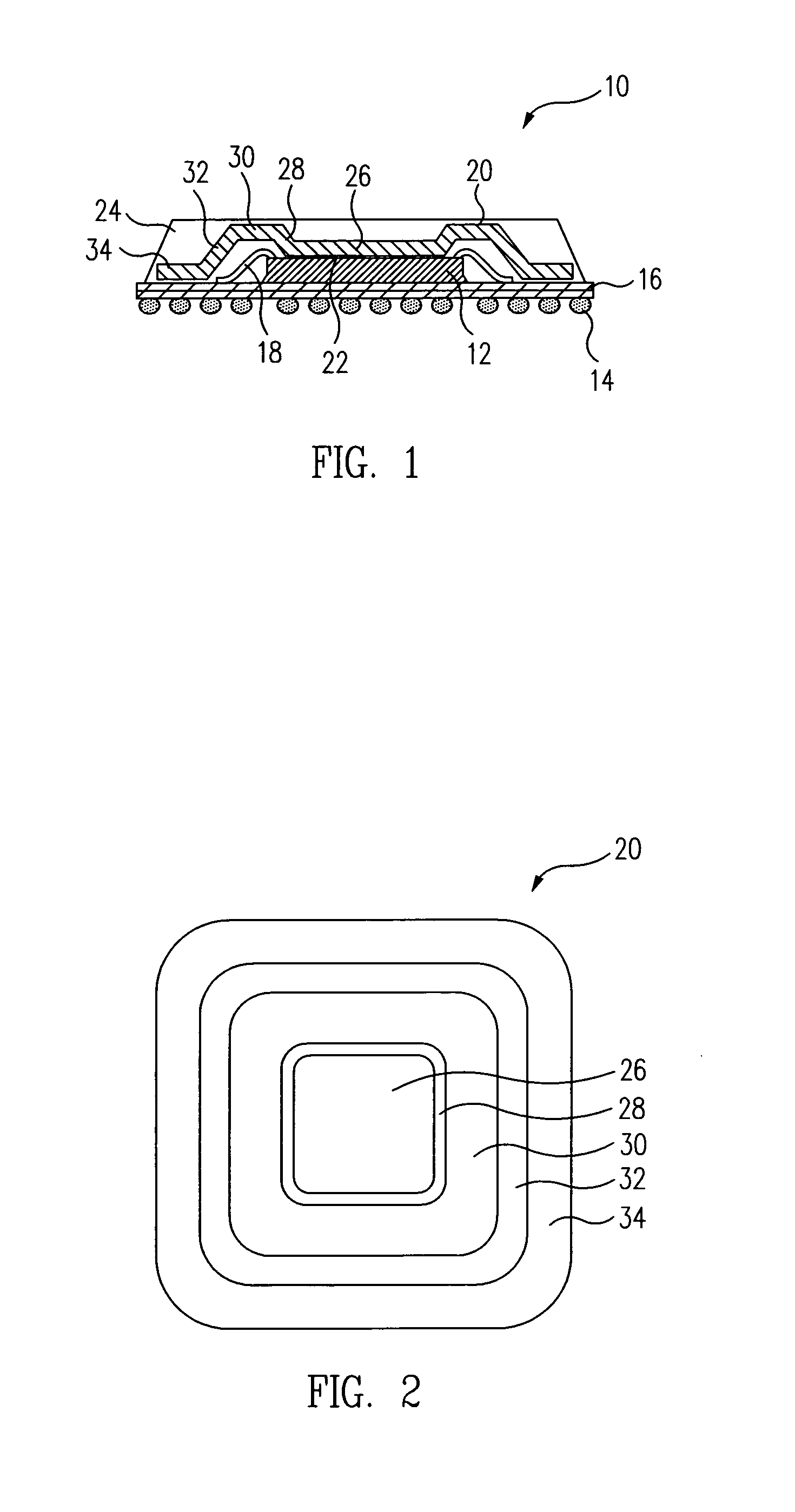
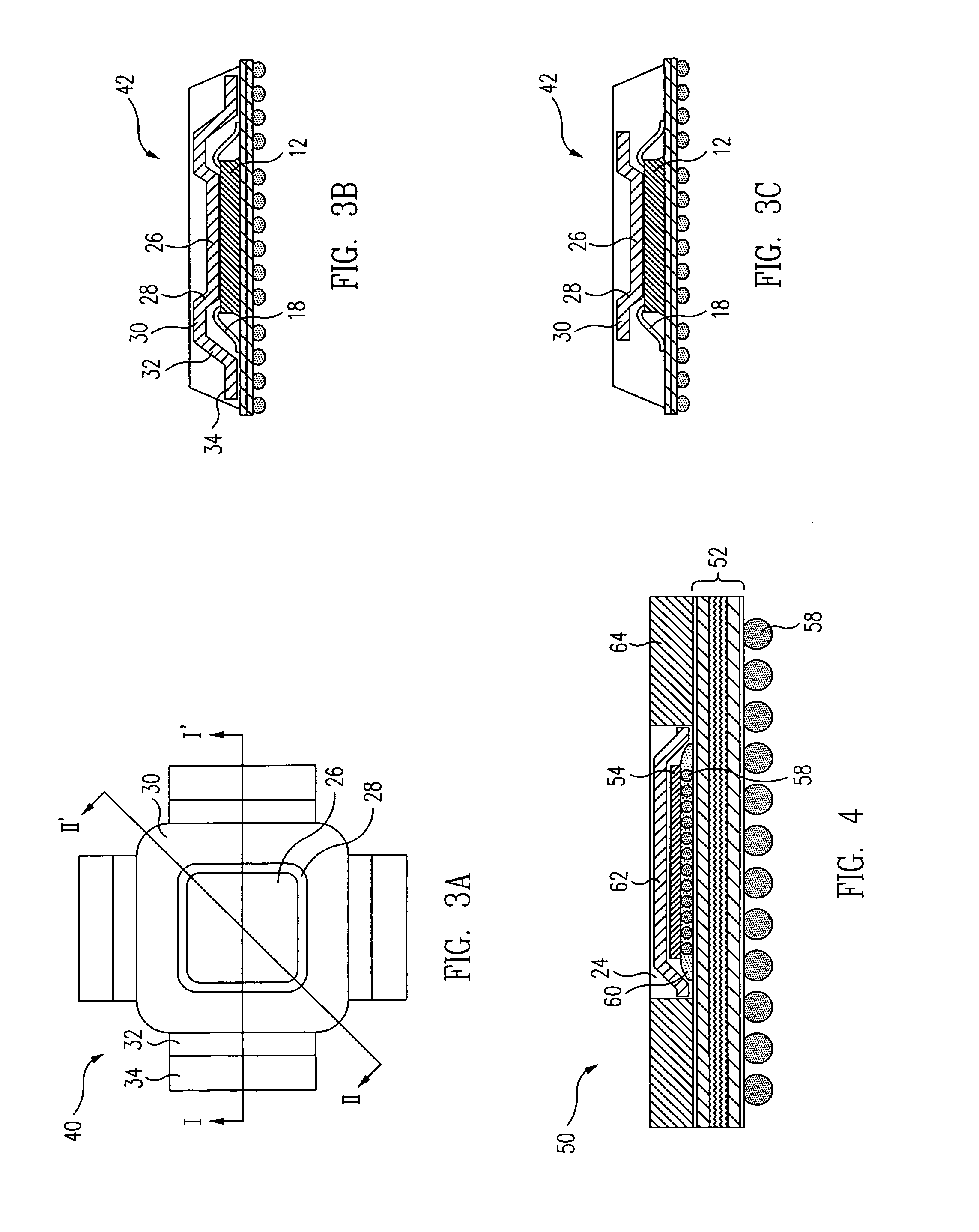
[0017]In accordance with one aspect of the present invention, a heat spreader or slug is attached directly to the face of a die in a die-up ball grid array (BGA) package and the heat slug, die, and bond wires completely encapsulated.

[0018]FIG. 1 is a side view of a BGA package 10 according to one embodiment of the present invention. BGA package 10 includes a semiconductor die 12 and an array of solder balls 14 electrically coupled to a substrate 16. Substrate 16 includes (not shown) multiple patterned dielectric and conductive layers, with vias and other interconnections providing connections between the various layers and to the top and bottom surfaces of the substrate. Die 12 is attached to the upper surface of substrate 16, such as by a silver epoxy, and electrically connected to traces on the upper surface of substrate 16, such as with bond wires 18. Solder balls 14 are set on the bottom surface of substrate 16 to provide electrical connection between external circuitry, such as...


PUM


Abstract

A heat slug or spreader is attached directly to a surface of the die in a ball grid array (BGA) package. The heat spreader roughly conforms to the topological profile of the die, underlying substrate, and electrical interconnections between the die and the substrate, such as bond wires. The outer portion of the heat spreader substantially cover the outer portion of the substrate, or alternatively, cover only those portions extending in laterally from the sides of the chip and not the corners. An encapsulant completely covers the heat spreader and die.

Description

FIELD OF THE INVENTION[0001]The present invention relates to semiconductor chip packages, and more specifically, to ball grid array packages with heat spreaders.BACKGROUND OF THE INVENTION[0002]In general, semiconductor packages are used to protect a semiconductor die in a package body and to provide connection points for connecting the packaged die to external devices and circuitry. Ball grid array (BGA) packages are currently used to handle the high density and high pin-count of semiconductor die. In a typical BGA package, the semiconductor die is mounted to the top surface of a printed circuit board (PCB) type substrate. The die is wire bonded to electrical traces on the top surface of the substrate. The bond wires and die are then typically encapsulated for protection. Solder balls are bonded to the electrical traces on the bottom surface of the substrate to provide electrical connection to an underlying device, such as a PCB.[0003]During operation of the integrated circuit, hea...

Claims


Application Information

Patent Timeline
Patent Type & Authority Patents(United States)
IPC IPC(8): H01L23/10H01L23/34
CPCH01L23/3128H01L23/4334H01L23/367H01L2224/16225H01L23/49816H01L2224/16H01L2224/48227H01L2224/73253H01L2224/83102H01L2224/92125H01L2924/01004H01L2924/15311H01L2924/16152H01L2924/3025H01L2224/32225H01L24/48H01L2224/73204H01L2924/00H01L2924/14H01L2924/00014H01L2924/181H01L2224/32245H01L2224/45099H01L2224/45015H01L2924/207
Inventor DARVEAUX, ROBERT F.HAMILTON, FREDERICK J. G.GUENIN, BRUCE M.DICAPRIO, VINCENT
Owner AMKOR TECH SINGAPORE HLDG PTE LTD
Learn More