Optical device, enclosure and method of fabricating

a technology of optical communication device and enclosure, applied in the field of enclosures for optical communication device, can solve the problems of time-consuming and costly multi-step machining process, and achieve the effect of minimizing the number of high-precision manufacturing steps and being better suited

Inactive Publication Date: 2006-10-31
BROADCOM INT PTE LTD
View PDF17 Cites 19 Cited by
  • Summary
  • Abstract
  • Description
  • Claims
  • Application Information

AI Technical Summary

Benefits of technology

[0013]An advantage of the invention is that it provides for an enclosure that is better suited for batch processing. For example, multiple lid portions can be formed into a single sheet of material and simultaneously joined to multiple base portions also formed in a single sheet of material. Thereafter lid and base pairs can be segmented from the whole to produce multiple individual devices.
[0014]Another advantage of the invention is that it provides for an enclosure that can be manufactured in a manner that minimizes the number of high precision manufacturing steps. For example, when multiple lid portions are simultaneously affixed to multiple base portions, as above, only one alignment step is required to align the multiple lid and base portions.

Problems solved by technology

This multi-step machining process is costly and time consuming, and is repeatedly performed for each lid and base.

Method used


Image

  • Optical device, enclosure and method of fabricating
  • Optical device, enclosure and method of fabricating
  • Optical device, enclosure and method of fabricating

Examples


Embodiment Construction

[0024]Before embodiments of the invention are described in detail, it should be understood that the invention is not limited to the exemplary embodiments or the process steps of the exemplary methods described herein. One of ordinary skill in the art will readily appreciate that the examples described herein may be applied to many devices and sub-devices that are utilized in technologies involving optics.

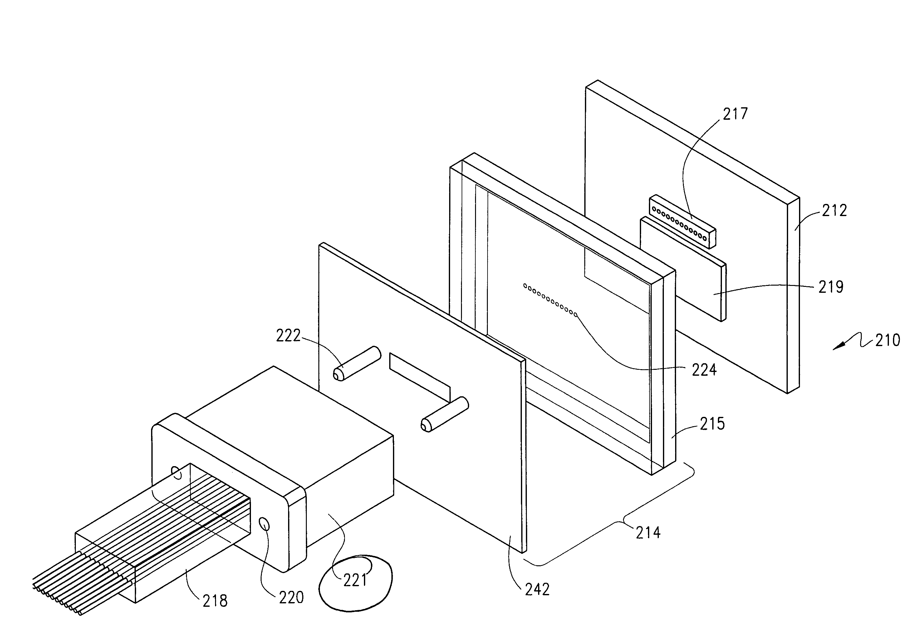
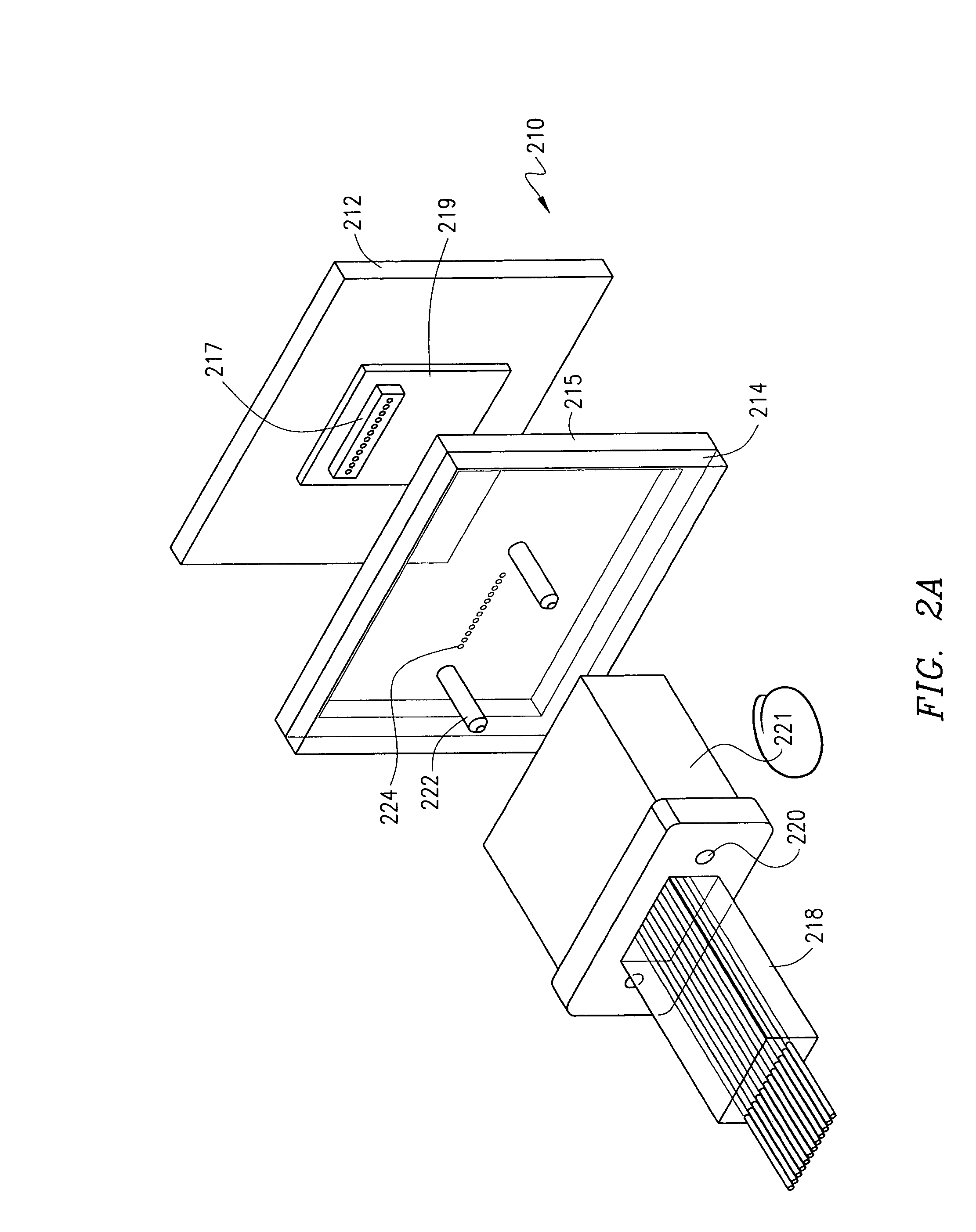
[0025]Referring first to FIGS. 2A and B, an exemplary optical interconnect module 210 constructed in accordance with this invention has at least a base portion 212 and a lid portion 214 which forms the enclosure. The base 212 has optical-electrical (eg. an electro-optical transducer) 217 and electrical components 219 (eg. an integrated circuit) thereon for interfacing the optical signal carried by the optical cable 218 with an electronic signal. Alternately, the base 212 may be integrally formed with the electrical components 219 and have optical-electrical components 219 mounted th...


PUM


Abstract

An enclosure for an optical communications device having a lid portion and a base portion. Alignment members adapted to interface with an optical connector are formed on the lid portion. The lid portion is affixed to the base portion with a portion of the communications components therebetween. Multiple base portions formed in a unitary piece of material and multiple lid portions formed in another unitary piece of material can be affixed to one another, and then separated into individual devices to minimize time spent aligning each base and lid portion.

Description

BACKGROUND OF THE INVENTION[0001]1. Technical Field of the Invention[0002]The present invention relates to optical communication devices, and more particularly enclosures for optical communications devices that provide alignment between the optical communications device and an optical cable.[0003]2. Description of Related Art[0004]An optical interconnect module is an optical-electrical device that enables an interface between optical communications systems and electrical communications systems. One or multiple optical fibers, bundled in an optic cable, are connected to the interconnect module to communicate with optical-electrical components of the interconnect module. The optical-electrical components interface data transmitted on the optical fibers to electrical communication systems or interface electrical communications systems to optical communications systems.[0005]An optical cable may need to be repeatedly connected and disconnected from the optical interconnect module. Becau...

Claims


Application Information

Patent Timeline
Patent Type & Authority Patents(United States)
IPC IPC(8): G02B6/36G02B6/32G02B6/42
CPCG02B6/32G02B6/4201G02B6/4249G02B6/3652G02B6/3692G02B6/3696G02B6/4224G02B6/4231G02B6/4256
Inventor GIBONEY, KIRK S.SIMON, JONATHAN
Owner BROADCOM INT PTE LTD
Why Eureka
Try Eureka