Image sensor pixel for global electronic shuttering

a global electronic shuttering and image sensor technology, applied in the field of solid-state image sensing devices, can solve problems such as increased fixed pattern noise, and achieve the effect of reducing pixel-related fixed pattern nois

Inactive Publication Date: 2006-10-31
OMNIVISION TECH INC
View PDF15 Cites 82 Cited by
  • Summary
  • Abstract
  • Description
  • Claims
  • Application Information

AI Technical Summary

Problems solved by technology

However, in the application areas of industrial cameras and high-frame rate recording, CMOS sensors have been handicapped by embodiments which employ row-by-row exposure controls which allows a slit shuttering mode that is not capable of simultaneous exposure of the entire CMOS pixel array.
However, the addition of the gate may cause increased fixed pattern noise due to non-optimal removal rates for charges stored within the photodetectors in the prior art devices.

Method used


Image

  • Image sensor pixel for global electronic shuttering
  • Image sensor pixel for global electronic shuttering
  • Image sensor pixel for global electronic shuttering

Examples


Embodiment Construction

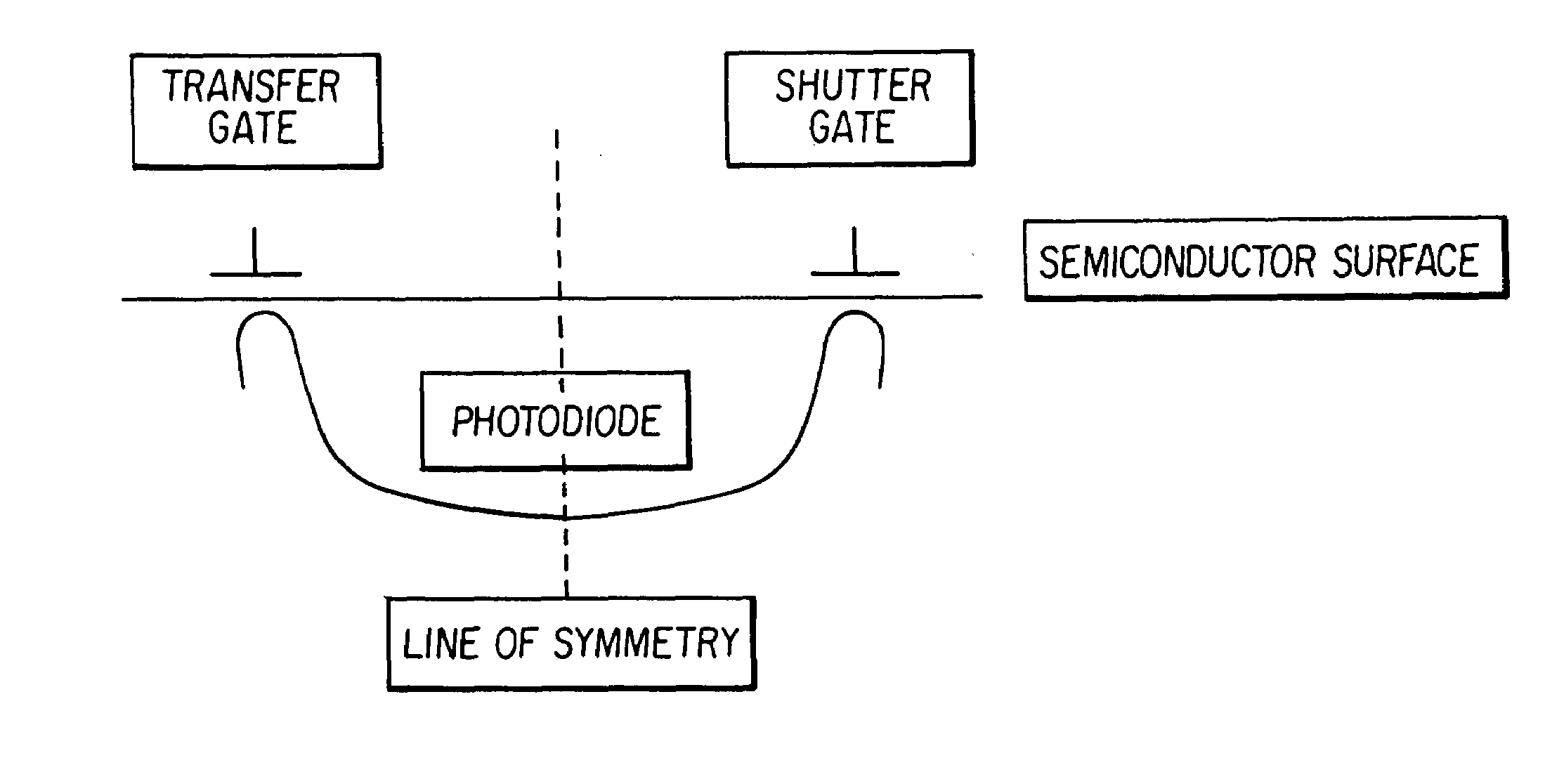
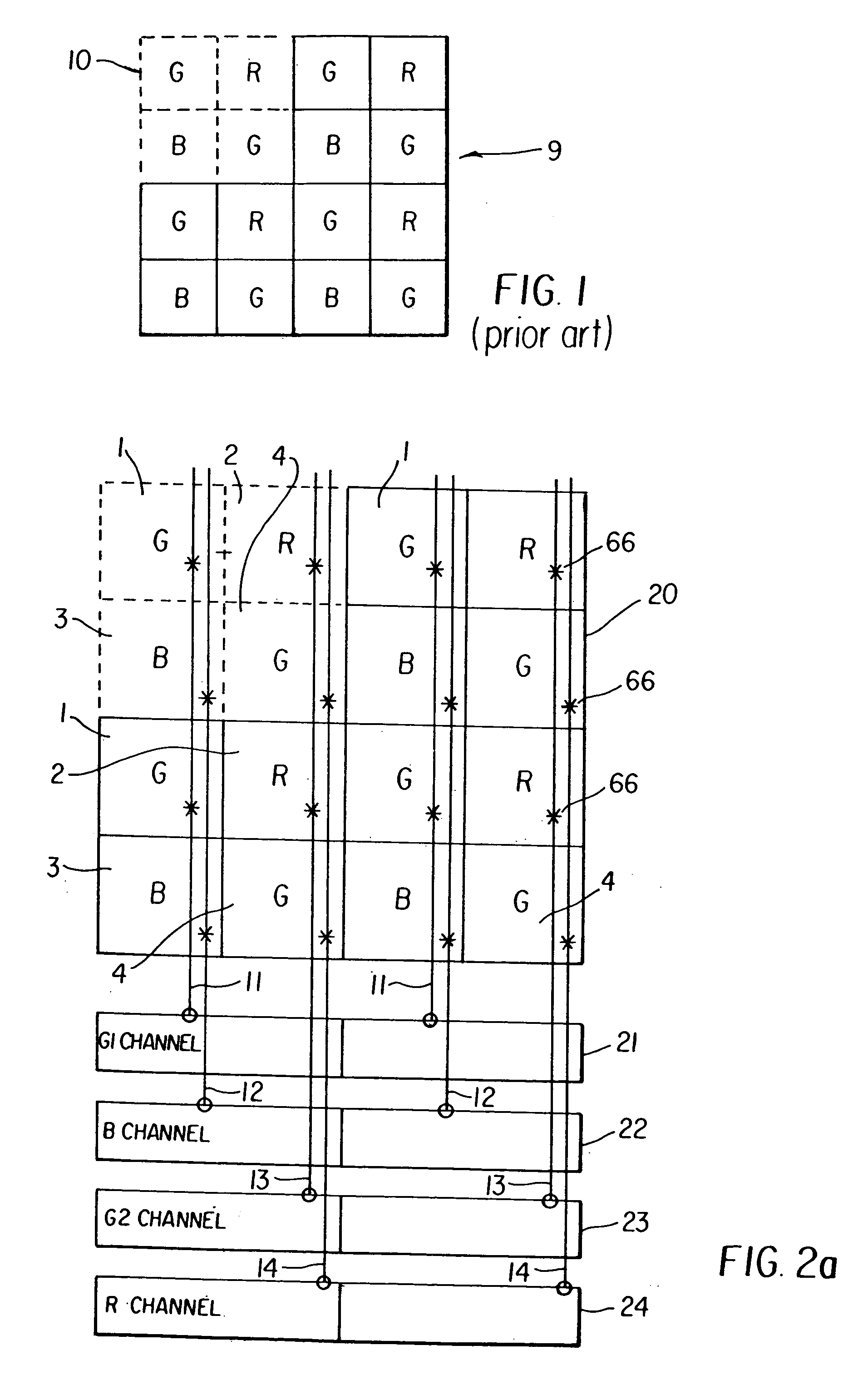
[0017]FIG. 1 is an example of a unit kernel 10 known as the Bayer CFA pattern design showing the four-pixel unit kernel 10 wherein G=green, R=red, and B=blue shows the color sensitivity of the pixels. The 2×2 pattern illustrated in the unit kernel 10 is a conventional prior-art image sensor construction. The photo-electric conversion means, such as a photo-diode, is formed in a semi-conductor layer during processing steps of forming various parts of the active device. These processing steps typically include photolithographical masking, ion implantation, diffusion and oxidation. The various parts of the active device are commonly a photodetector using either photo-diode or photogate technology, source / gate / drain of Metal Oxide Semiconductor Field Effect Transistors (MOSFET's), and isolation regions. Additionally, poly-silicon and silicon oxide layers are deposited, patterned and formed on the semi-conductor layers to form transistors. Finally, layers of isolation dielectric are over...


PUM


Abstract

A pixel design for CMOS image sensors that has a high frame rate potential and, therefore, provides motion capture capabilities. The pixel is designed for global electronic shuttering so every pixel is exposed simultaneously to images incident upon the pixel array plane. The present invention has the advantages of: (1) Allowing the accommodation of changes in the pixel output groupings for different monochrome output format or CFA patterns with only changes in metal routing layers; (2) allowing true electronic shuttering to image moving scene with all the pixels having the same capture time windows; and (3) providing a symmetric global shutter gate and transfer gate to minimize pixel related fixed pattern noise. The pixel architecture provides for a CMOS based, active pixel image sensor comprising an array of pixels formed in rows and columns, with each of the pixels containing at least one active circuit element. There are a plurality of output channels formed such that each of the output channels are operatively connected to a subset of pixels wherein each of the pixel have an attribute that is the same. The pixel architecture also provides an output gate region and a shutter gate region that are symmetric about the center of the pixel. By arranging the shutter and transfer gates, a symmetric manner about the center of the pixel, a more efficient transfer of electrons to these gates is provided. A Pixel Output Bus structure allows configurable connections to column-wise signal busses that provide parallel output channels.

Description

BACKGROUND OF THE INVENTION[0001]1. Field of the Invention[0002]The present invention relates to the field of solid-state image sensing devices and, more specifically, to CMOS based active pixel sensors.[0003]2. Description of the Prior Art[0004]CMOS active pixel image sensors have been rapidly developed to supplement and replace charge-coupled devices in many applications. CMOS image sensors have advantages in low-power operation as well as the higher integration capabilities for on-chip signal processing and control functions that are available with CMOS technology. Therefore, the technology is suitable for many consumer applications, including low-cost portable imaging devices. CMOS based sensors allow for the incorporation of numerous functions onto a single chip. Various prior art references have disclosed Active Pixel Sensors based on CMOS that employ sense node connected to photodetectors through transfer gates. Typically a reset gate is provided that can be used for shutteri...

Claims


Application Information

Patent Timeline
Patent Type & Authority Patents(United States)
IPC IPC(8): H04N3/14H01L27/146H01L31/02H04N5/351H04N5/374H04N9/04H04N9/07
CPCH01L27/14603H04N5/351H04N5/3742H04N9/045H01L27/14621H01L27/14645H04N25/50H04N25/70H04N25/767H04N25/134H04N25/136
Inventor LEE, PAUL P.
Owner OMNIVISION TECH INC
Why Eureka
Try Eureka