Processes for coating photoconductors

a technology of photoconductors and coatings, applied in electrographic processes, corona discharge, instruments, etc., can solve the problems of easy disturbance or destruction, toner image, loose powdered form, etc., and achieve the disadvantages inherent in the dip coating process

Inactive Publication Date: 2006-11-07
XEROX CORP
View PDF25 Cites 7 Cited by
  • Summary
  • Abstract
  • Description
  • Claims
  • Application Information

AI Technical Summary

Benefits of technology

[0017]This invention provides methods and apparatuses for coating objects without requiring dip coating. The methods and apparatuses offer uniform, fast coating by dispensing coating material onto a rotated object in a helical pattern. In one aspect of the invention, i.e., the coating apparatus includes a coating device that dispenses coating material, a rotation device that rotates an object to be coated, and a movement device that relatively moves the c

Problems solved by technology

The visible toner image is then in a loose powdered form and can be easily disturbed or destroyed.
However, there are disadvantages inherent in the dip coating process.
Additionally, the coating material is restricted to materials that have a relatively long “pot life” , i.e., materials that can stay in a dip coating tank for a relatively long time without hardening or otherwise becoming unusable.
Another disadvanta

Method used


Image

  • Processes for coating photoconductors
  • Processes for coating photoconductors
  • Processes for coating photoconductors

Examples


Embodiment Construction

[0026]In embodiments of the present invention there is provided a process comprising:

[0027]providing a cylindrical substrate rotating about the long axis;

[0028]applying at least one coating layer with a direct writing applicator on the outer surface of the rotating substrate; and

[0029]curing the resulting coated layer or layers.

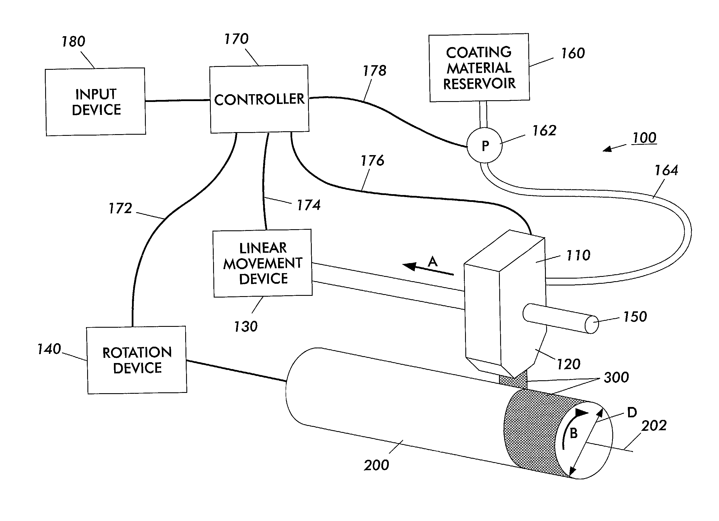
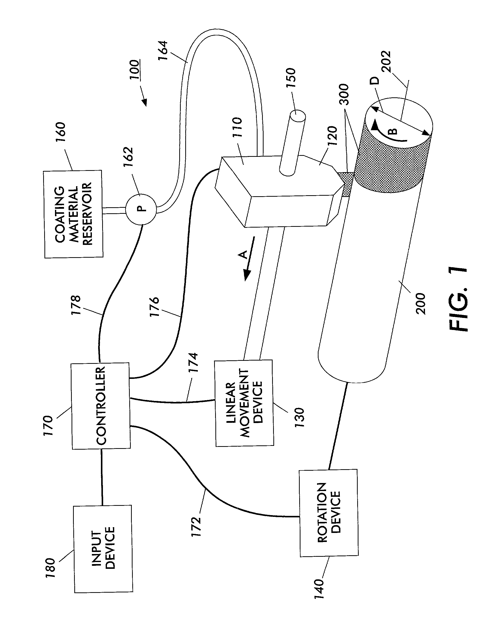
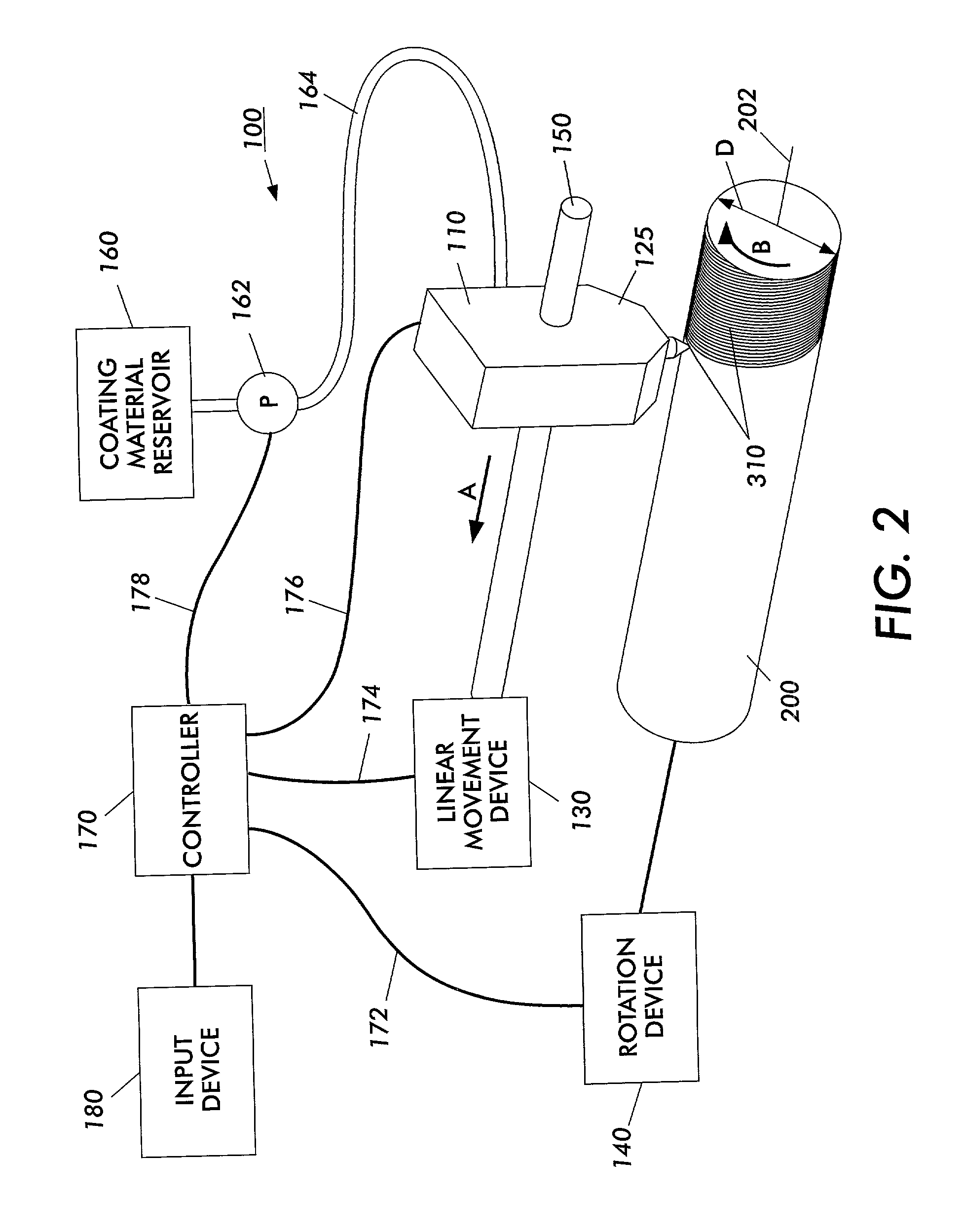
[0030]This invention provides methods and apparatuses for coating objects without requiring dip coating. The methods and apparatuses offer uniform, fast coating by dispensing coating material onto a rotated object in a helical pattern. FIG. 1 shows an exemplary coating apparatus 100 according to this invention.

[0031]The coating apparatus 100 includes a coating device 110, a linear movement device 130 and a rotation device 140. The coating device 110 is in operative connection with a guide / driving device 150, which in turn is in operative connection with the linear movement device 130. For example, the guide / driving device 150 may include a rotating threaded m...


PUM

PropertyMeasurementUnit
Thicknessaaaaaaaaaa
Thicknessaaaaaaaaaa
Widthaaaaaaaaaa

Abstract

A process including: providing a cylindrical substrate rotating about the long axis; applying at least one coating layer with a direct writing applicator on the outer surface of the rotating substrate; and curing the resulting coated layer or layers. The use of a direct writing applicator provides precision in the dispensing of organic photoconductor coating layers with respect to line width and line thickness.

Description

CROSS REFERENCE TO COPENDING APPLICATIONS AND RELATED PATENTS [0001]This application is a continuation-in-part of and claims priority under 35 U.S.C. § 120 to U.S. application Ser. No. 09 / 953,526, now U.S. patent No. 6,706,315, filed on Sep. 17, 2001.[0002]Attention is directed to commonly assigned copending applications: U.S. Pat. No. 6,214,513 discloses a coating process for the fabrication of organic photoreceptors which process employs an electrically conductive single slot die biased to allow an electric field between the die and the ground plane on the photoreceptor substrate. The homogenous coating dispersion is fed through the die at a predetermined gap and rate to control coating thickness at the same time that an electric field is applied. The formulation, rheology, particle mobility, coating speed, electric field and the like are controlled so that the photogenerator particles migrate to the substrate in the dwell time defined by the coating die region.[0003]U.S. Ser. No....

Claims


Application Information

Patent Timeline
IPC IPC(8): B05D5/06B05C5/02B05D1/26G03G5/05
CPCB05C5/0254G03G5/0525B05D1/26B05C5/0258
Inventor HAMMOND, JOHN M.TRABOLD, THOMAS A.
Owner XEROX CORP
Why Eureka
Try Eureka