Image sensor circuits including sampling circuits used therein for performing correlated double sampling

Inactive Publication Date: 2006-11-07
QUALCOMM INC
View PDF30 Cites 44 Cited by
  • Summary
  • Abstract
  • Description
  • Claims
  • Application Information

AI Technical Summary

Benefits of technology

[0010]In the context of an image sensor circuit having an array of pixels including light sensing nodes at each of which a change in voltage can be imparted by exposure to a light source, the present invention further provides a method for obtaining output signals representing the voltage changes at the light sensing nodes in order to obtain image data, comprising: at each said pixel providing an amplifier circuit with an input driven by the voltage on the respective light sensing node to produce an amplifier output; providing a sample and hold circuit coupled to selectively receive the amplifier output of a said pixel amplifier circuit in the a

Problems solved by technology

The present CCD imagers have a number of good features including high image quality and low noise characteristics; however, there are also several limitations which are inherent to CCD's.
The specialized process utilized to produce CCD imagers is not well suited to forming driving and processing circuitry used in conjunction with the CCD image sensing array.
Thus, it is necessary to implement those functions on secondary integrated circuit chips, which increases the complexity and cost of the CCD imaging system.
The sensitive clocking requirements of CCD's adds further complexity and result

Method used


Image

  • Image sensor circuits including sampling circuits used therein for performing correlated double sampling
  • Image sensor circuits including sampling circuits used therein for performing correlated double sampling
  • Image sensor circuits including sampling circuits used therein for performing correlated double sampling

Examples


Embodiment Construction

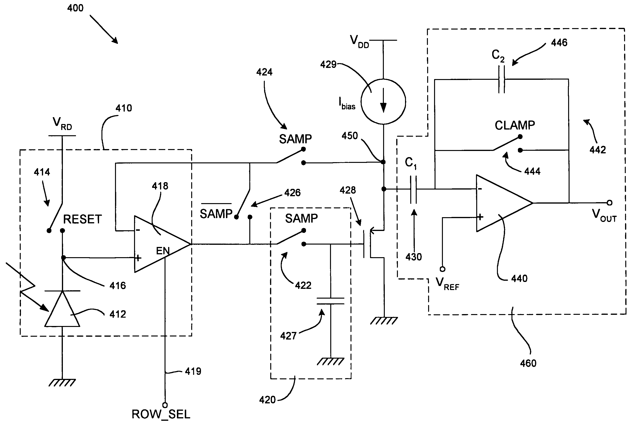
[0022]A method and apparatus for sampling pixel signal levels in a CMOS image sensor circuit is disclosed herein. In the following description, for purposes of explanation, specific nomenclature and specific implementation details are set forth to provide a thorough understanding of the present invention. However, it will be apparent to one skilled in the art that these specific details are not required in order to practice the present invention. For example, the present invention has been described with reference to N-Well process technologies. However, the same teachings can easily be applied to other types of process technologies.

A CMOS Image Sensor Array

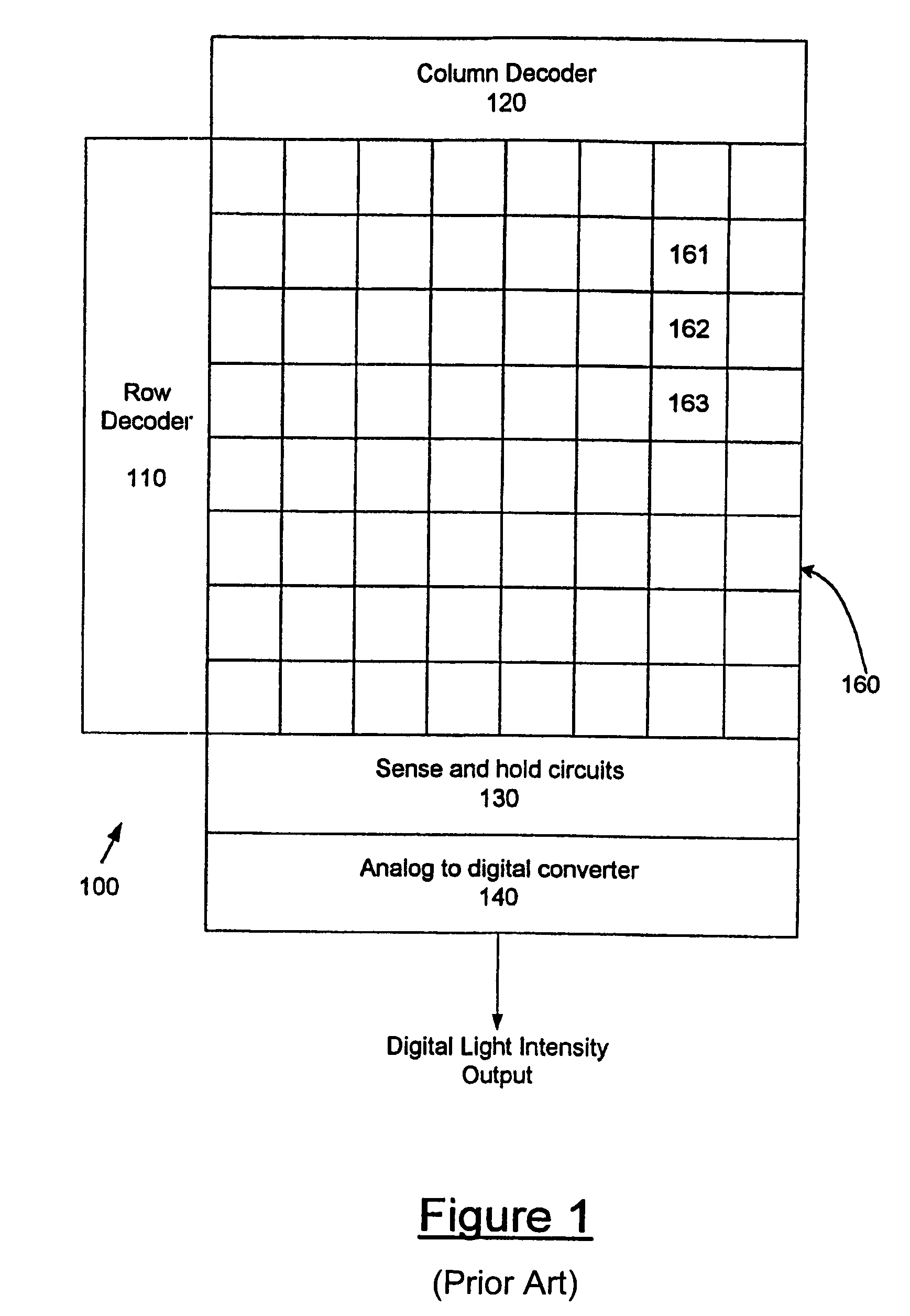
[0023]FIG. 1 is a block diagram of a circuit 100 having a typical two-dimensional CMOS image sensor array 160. Each element in the array 160 (such as array elements 161, 162, and 163) is an individual CMOS image sensor circuit. The individual CMOS image sensor circuits are also known as pixel circuits.

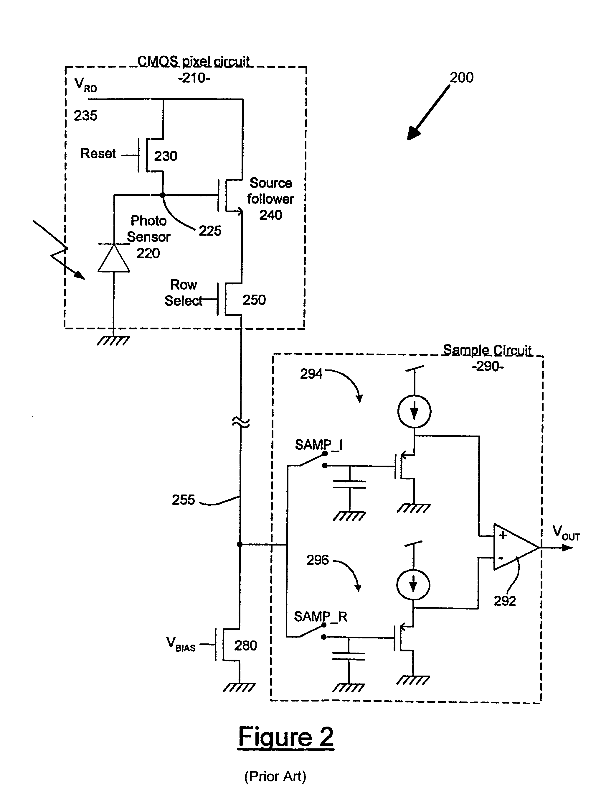
[0024]The CMOS image sensor ...


PUM


Abstract

A CMOS image sensor circuit includes an array of sensing elements which integrate electrical charge according to the light intensity thereon. In order to measure the accumulated charge voltage at the individual sensing elements, and thus obtain the image data from the array, a sampling circuit is provided. The sampling circuit operates using a high-gain amplification stage and an auto-zero amplifier to perform correlated double sampling, which enables non-linear influences which may arise in the array to be reduced in the measuring process. The sampling circuit can also include a sample and hold circuit arranged to account for a feed-through effect arising from pre-charge circuitry in the sensing elements. The sample and hold circuit can be included within the feed-back loop of the high-gain amplification stage for further increases in linear performance.

Description

FIELD OF THE INVENTION[0001]The present invention relates to the field of image sensor circuits. In particular, the present invention relates to a method and apparatus for sampling pixel signal levels in a CMOS image sensor.BACKGROUND OF THE INVENTION[0002]Semiconductor image sensing devices are finding widespread application with the increased use of digital still cameras and digital video cameras. Charge coupled device (CCD) technology has hitherto dominated the market for such imagers. The present CCD imagers have a number of good features including high image quality and low noise characteristics; however, there are also several limitations which are inherent to CCD's. The specialized process utilized to produce CCD imagers is not well suited to forming driving and processing circuitry used in conjunction with the CCD image sensing array. Thus, it is necessary to implement those functions on secondary integrated circuit chips, which increases the complexity and cost of the CCD i...

Claims


Application Information

Patent Timeline
IPC IPC(8): H04N3/14H04N5/217H04N5/335H04N5/365H04N5/374H04N5/378
CPCH04N5/335H04N25/00
Inventor BREHMER, KEVIN E.HARRIS, BRANNON
Owner QUALCOMM INC
Why Eureka
Try Eureka