
Method to realize fast silicon-on-insulator (SOI) optical device

a technology of silicon-on-insulator and optical device, applied in the field of photonic devices, can solve the problem of limited high-operation frequency of silicon-based electrical semiconductor devi

Inactive Publication Date: 2006-11-07
MICRON TECH INC
View PDF24 Cites 10 Cited by
  • Summary
  • Abstract
  • Description
  • Claims
  • Application Information

AI Technical Summary

Benefits of technology

This approach enables faster transition between 'ON' and 'OFF' states, achieving high-speed optical modulation and attenuation, and dynamic gain equalization, thereby improving signal processing speed and reducing optical loss in photonic integrated circuits.

Problems solved by technology

It is well known that the highest operational frequency a silicon based electrical semiconductor device may have is limited by the speed at which the device switches.

Method used


Image

  • Method to realize fast silicon-on-insulator (SOI) optical device
  • Method to realize fast silicon-on-insulator (SOI) optical device
  • Method to realize fast silicon-on-insulator (SOI) optical device

Examples


Embodiment Construction

[0019]A fast optical device on an SOI platform is described in detail herein. In the following description, numerous specific details, such as particular processes, materials, devices, and so forth, are presented to provide a thorough understanding of embodiments of the invention. One skilled in the relevant art will recognize, however, that the invention can be practiced without one or more of the specific details, or with other methods, components, etc. In other instances, well-known structures or operations are not shown or described in detail to avoid obscuring embodiments of various embodiments of the invention.

[0020]Some parts of the description will be presented using terms such as waveguide, silicon, irradiation, doping, implantation, and so forth. These terms are commonly employed by those skilled in the art to convey the substance of their work to others skilled in the art.

[0021]Other parts of the description will be presented in terms of operations performed by a computer...


PUM

PropertyMeasurementUnit
wavelengthaaaaaaaaaa

Abstract

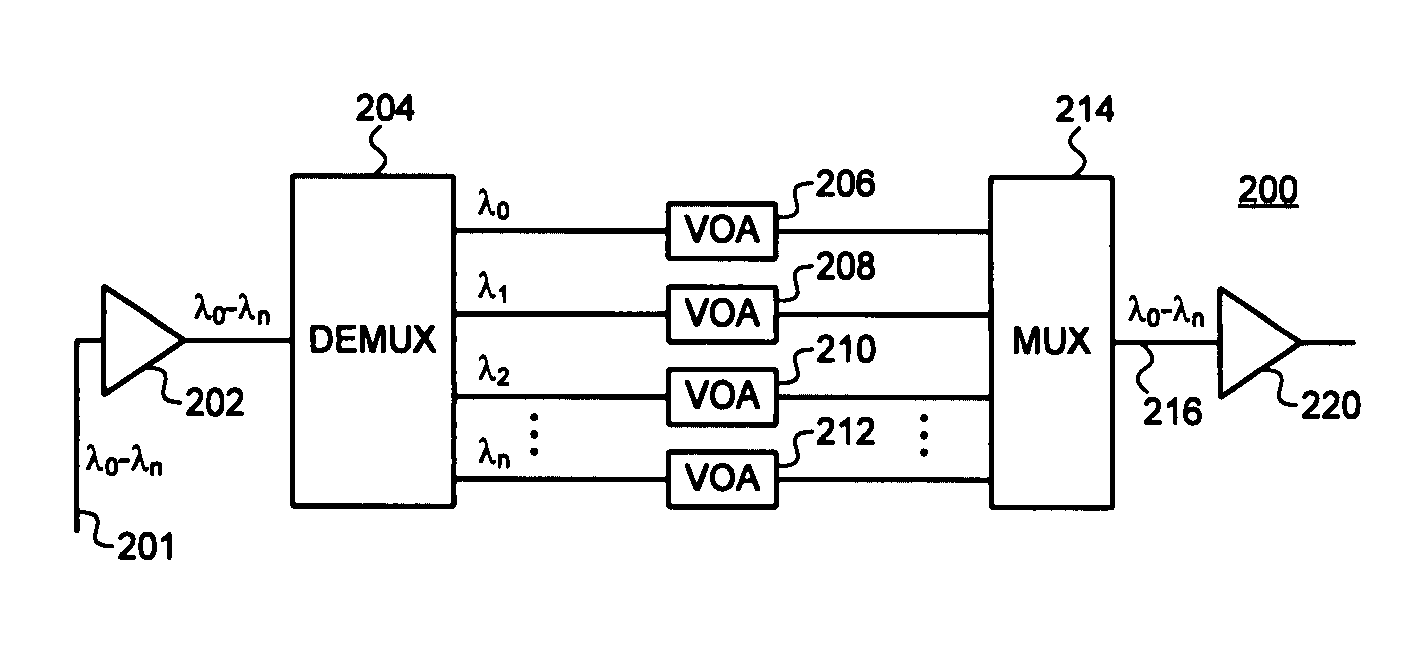
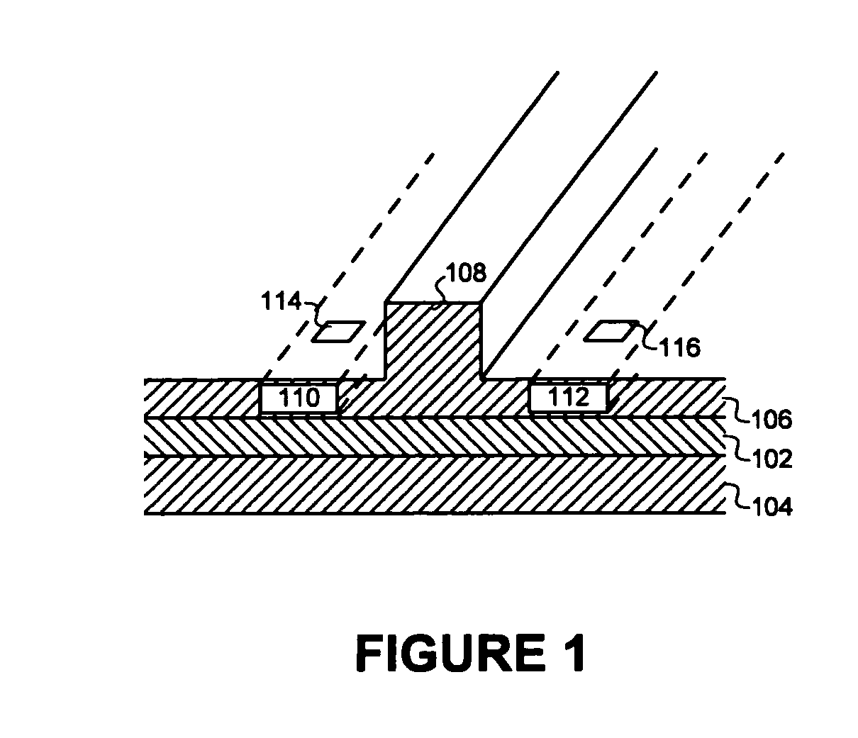
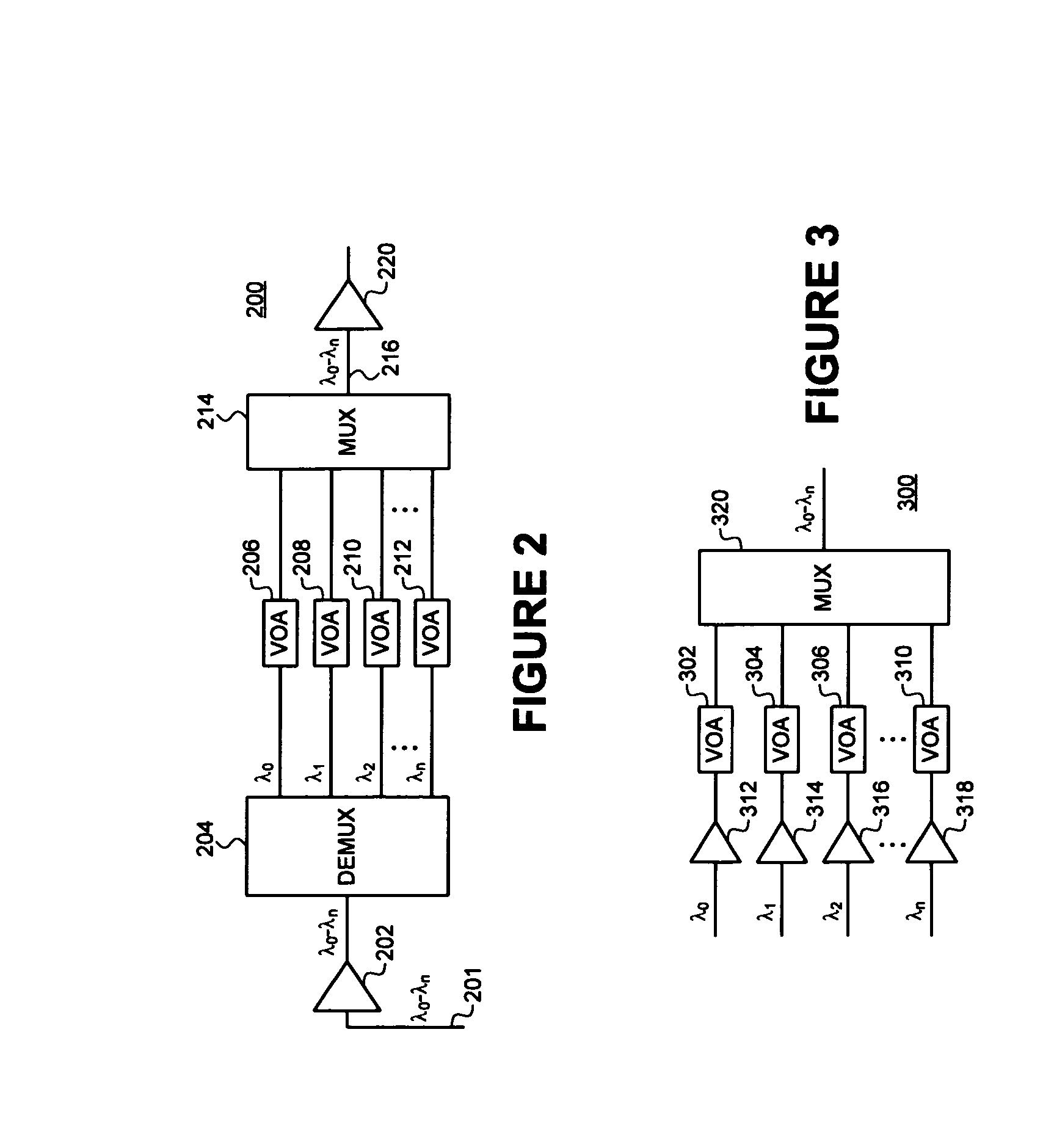
A fast silicon-on-insulator (SOI) waveguide-based optical device enhanced with minority charge carrier lifetime modifiers enables faster modulation speeds in optical attenuators, optical intensity / phase-modulators, and optical switches whose operation principles are based on free-carrier injection into a waveguide. The waveguide is doped with gold (Au) or platinum (Pt) such that when a drive voltage (applied to the device) is turned off, the minority charge carriers rapidly annihilate because gold doping reduces the minority carrier lifetime, which improves transient characteristics of the optical device. Integration of the fast active device with passive devices such as WDM demultiplexers / multiplexers on the SOI optical waveguide platform enables realization of monolithic integrated optical components for advanced functionality such as dynamic spectral equalization.

Description

CROSS-REFERENCE TO RELATED APPLICATIONS[0001]This application is a Continuation of U.S. application Ser. No. 10 / 061,981, filed Jan. 31, 2002.BACKGROUND OF THE INVENTION[0002]1. Field of the Invention[0003]The present invention is related to photonic devices and, in particular to integrated optical circuits.[0004]2. Background Information[0005]Silicon, as an electronic material, is widely used to realize electronic integrated circuits. Over ninety percent of integrated circuits fabricated worldwide use silicon as the starting material. It is well known that the highest operational frequency a silicon based electrical semiconductor device may have is limited by the speed at which the device switches. The switching speed of a bipolar semiconductor device is related to the “minority carrier life times” in the active area of the silicon crystals that makes the device work. A minority carrier is one whose equilibrium concentration (in silicon) is less than the majority carrier. For exampl...

Claims


Application Information

Patent Timeline
Patent Type & Authority Patents(United States)
IPC IPC(8): G02B6/12G02F1/025
CPCG02F1/025G02B2006/12164
Inventor YEGNANARAYANAN, SIVASUBRAMANIAMNAYDENKOV, MIKHAIL
Owner MICRON TECH INC
Learn More