ESD design, verification and checking system and method of use

a technology of esd and design system, applied in the direction of software simulation/interpretation/emulation, instruments, program control, etc., can solve the problems of esd, high risk of damage to integrated circuits, and less ability to discharge static electricity,

Inactive Publication Date: 2006-11-07
INT BUSINESS MASCH CORP
View PDF6 Cites 25 Cited by
  • Summary
  • Abstract
  • Description
  • Claims
  • Application Information

AI Technical Summary

Problems solved by technology

In particular, many integrated circuits are highly susceptible to damage from the discharge of static electricity, even at levels which can neither be seen nor felt.
The discharge of static electricity, or ESD, has become a critical problem for the electronics industry.
Device failures are not always immediately catastrophic, but often the device is weakened thus less able to withstand normal operating stresses and, hence, may result in a reliability problem.
This design practice does not allow for the flexibility needed for RF applications.
A difficulty in the design of RF ESD solutions is that traditionally, specific designs are fixed in size in order to achieve verifiable ESD results for a technology.
The difficulty with analog and RF technology is that a wide range of circuit applications exists where one ESD size structure is not suitable due to loading of the circuit.
A second issue is that the co-synthesis of the circuits must be done to properly evaluate the RF performance objectives.
A third issue for RF mixed signal designs, there are analog and digital circuits.
Additional difficulties are encountered from the different views of an ESD circuit (e.g., symbol, circuit schematic and graphical representations) and the mapping from the graphical to circuit representations, circuit schematic representation to the graphical representation in the environment of a variable ESD circuit sizes.

Method used


Image

  • ESD design, verification and checking system and method of use
  • ESD design, verification and checking system and method of use
  • ESD design, verification and checking system and method of use

Examples


Embodiment Construction

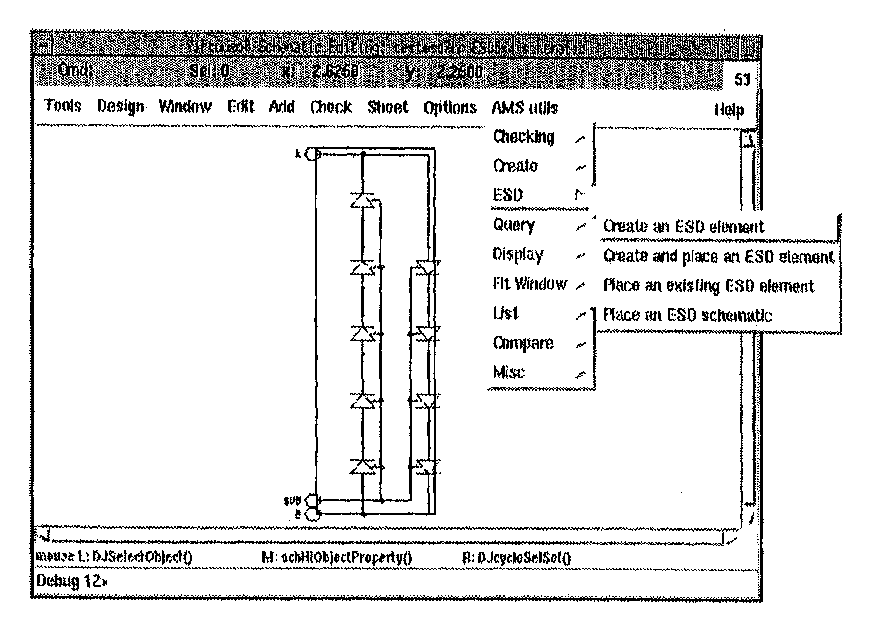
[0050]The invention relates to a system and method for designing ESD elements (circuits). The invention also relates to verification and checking of such circuits, ensuring the robustness of the ESD circuit and accompanying design. In the design phase, layout and circuit schematics are auto-generated with the user capable of varying the number of parameters, i.e., elements, in the circuit. The ESD design system allows for change of circuit topology as well as structure size in an automated fashion, without additional design work. Interconnects and wiring between the circuit elements are also auto-generated with use of the invention.

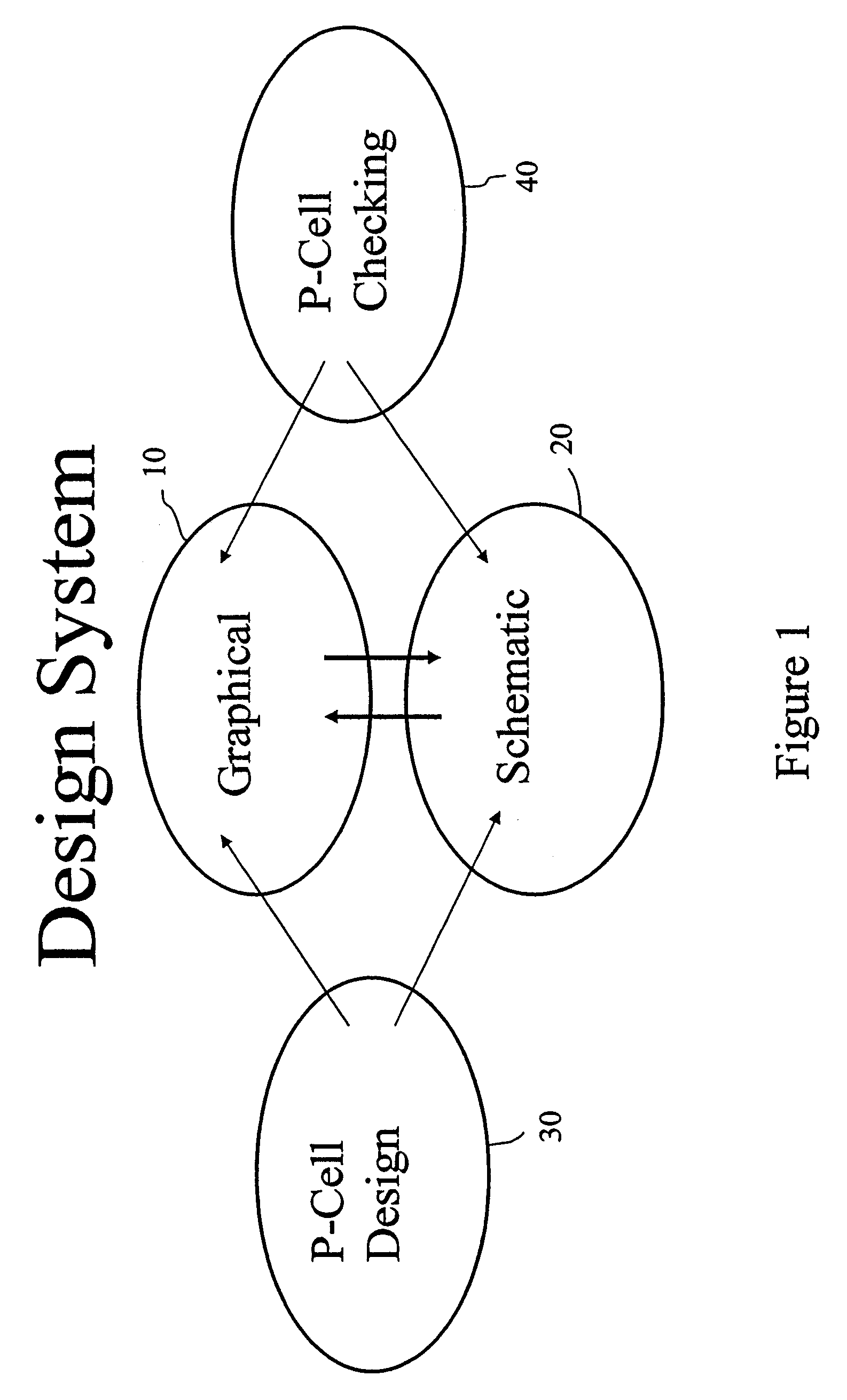
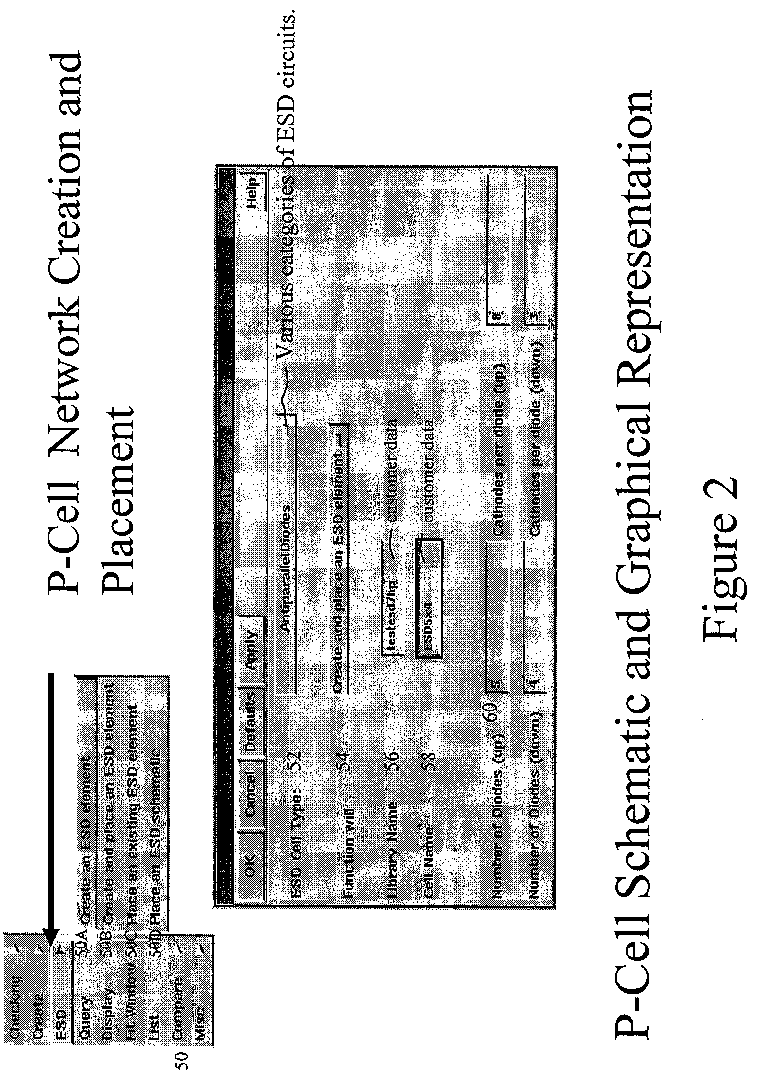
[0051]The invention is suitable for an ESD CAD strategy that provides design flexibility, RF characterization and models of ESD elements, automation, and choice of ESD network type. The environment employed may use a hierarchical system of parameterized cells, referred to as “p-cells”, which are constructed into higher level ESD networks. The parameterize...


PUM


Abstract

A computerized method and system for designing, verification and checking of the electrostatic discharge (ESD) protection circuits and their implementation in a integrated computer chip design where the computer chip comprises of electronic circuits designed in a parameterized cell design system, pads, interconnects and the ESD system uses a hierarchical system of parameterized cells (p-cells) which are constructed into higher level ESD networks. Lowest order p-cells pass user defined parameters to higher order p-cells to form an ESD protection circuit meeting design criteria. Ones of the p-cells are “grow-able” such that they can form repetition groups of the underlying p-cell element to accommodate the design parameters. Layout and circuit schematics are auto-generated with the user varying the number of elements in the circuit by adjusting the input parameters. The circuit topology automation allows for the customer to auto generate new ESD circuits and ESD power clamps without additional design work.

Description

BACKGROUND OF INVENTION[0001]1. Field of the Invention[0002]The invention generally relates to a electrostatic discharge (ESD) design system and method of use and, more particularly, to an automated computer aided design (CAD) system and method of use for design, verification and checking of ESD circuits for a given application.[0003]2. Background Description[0004]As electronic components become smaller and smaller along with the internal structures in integrated circuits, it is becoming easier to either completely destroy or otherwise impair electronic components. In particular, many integrated circuits are highly susceptible to damage from the discharge of static electricity, even at levels which can neither be seen nor felt. This is typically referred to as electrostatic discharge (ESD), in which the transfer of an electrostatic charge occurs between bodies at different electrostatic potentials (voltages) caused by direct contact or induced by an electrostatic field.[0005]The dis...

Claims


Application Information

Patent Timeline
Patent Type & Authority Patents(United States)
IPC IPC(8): G06F17/50G06F9/455
CPCG06F17/5036G06F30/367
Inventor COLLINS, DAVID S.JORDAN, DONALD L.STRANG, SUE E.VOLDMAN, STEVEN H.
Owner INT BUSINESS MASCH CORP
Why Eureka
Try Eureka