Method for fabricating transistor gate structures and gate dielectrics thereof

a transistor and gate dielectric technology, applied in the field of semiconductor devices, can solve the problems of limited limited ability to form thin oxide films with uniform thickness, and electrical and physical limitations of the extent to which the thickness of siosub>2 /sub>gate dielectrics can be reduced, so as to improve the thermal stability of the deposited material

Active Publication Date: 2006-11-14
TEXAS INSTR INC
View PDF19 Cites 64 Cited by
  • Summary
  • Abstract
  • Description
  • Claims
  • Application Information

AI Technical Summary

Benefits of technology

[0011]One aspect of the invention combines a post-deposition nitridation process with two or more post-deposition anneal operations, where one is oxidizing and one is non-oxidizing. In accordance with this aspect, a method is provided for treating a deposited high-k gate dielectric layer during fabrication of a semiconductor device. The method comprises nitriding a deposited high-k gate dielectric layer, performing a first anneal in a non-oxidizing ambient, and performing a second anneal in an oxidizing ambient. In one implementation, the nitridation is done prior to both the anneal processes, with the non-oxidizing anneal being done last (e.g., prior to depositing the gate electrode material). In another implementation, the non-oxidizing anneal is done prior to nitridation. Either implementation may be used in conjunction with nitrogen-containing high-k materials or with materials initially deposited with no nitrogen content, wherein the nitridation step may improve thermal stability of the deposited material in either case.

Problems solved by technology

However, there are electrical and physical limitations on the extent to which thickness of SiO2 gate dielectrics can be reduced.
For example, very thin SiO2 gate dielectrics are prone to large gate tunneling leakage currents resulting from direct tunneling through the thin gate oxide.
In addition, there are conventional limitations on the ability to form such thin oxide films with uniform thickness.
Furthermore, thin SiO2 gate dielectric layers provide a poor diffusion barrier to dopants, for example, and may allow high boron dopant penetration into the underlying channel region of the silicon during fabrication of the source / drain regions.
While the macroscopic composition (e.g., stoichiometry) of these materials may be controlled to a certain extent during such deposition processes, stoichiometric composition variations within the film may degrade device performance.
In addition, the above deposition techniques often create high-k dielectric films having point defects that affect transistor performance.
Such defects may include oxygen vacancies, and / or other point defects affecting leakage through the gate dielectric.
Furthermore, certain deposition processes (e.g., CVD, ALD, etc.) may introduce impurities (e.g. Cl, C, OH, H, etc.) into the deposited high-k dielectric film, which also degrade device performance.
Moreover, the deposited film may not be of optimal density, wherein sub par performance may result.

Method used


Image

  • Method for fabricating transistor gate structures and gate dielectrics thereof
  • Method for fabricating transistor gate structures and gate dielectrics thereof
  • Method for fabricating transistor gate structures and gate dielectrics thereof

Examples


Embodiment Construction

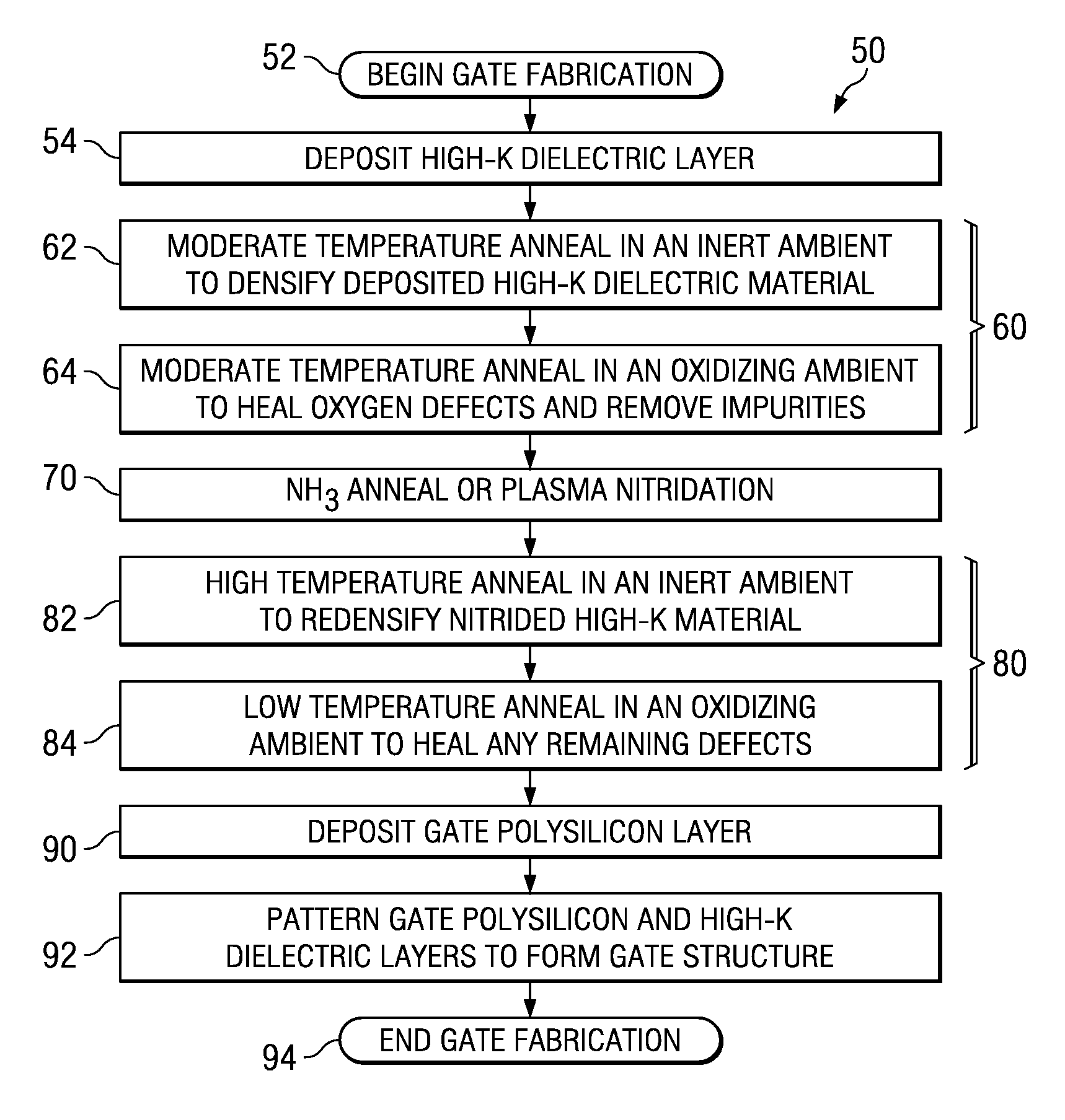
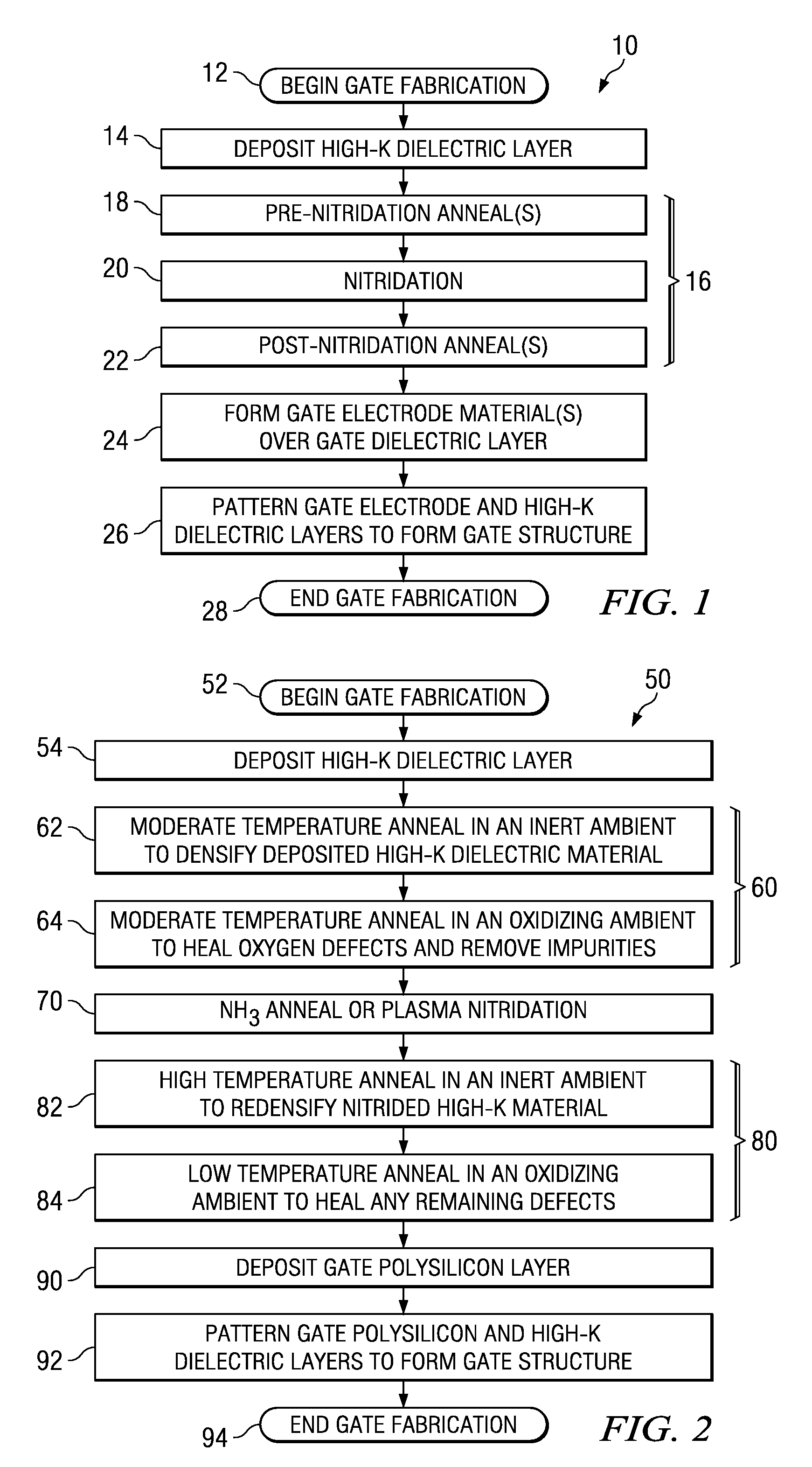
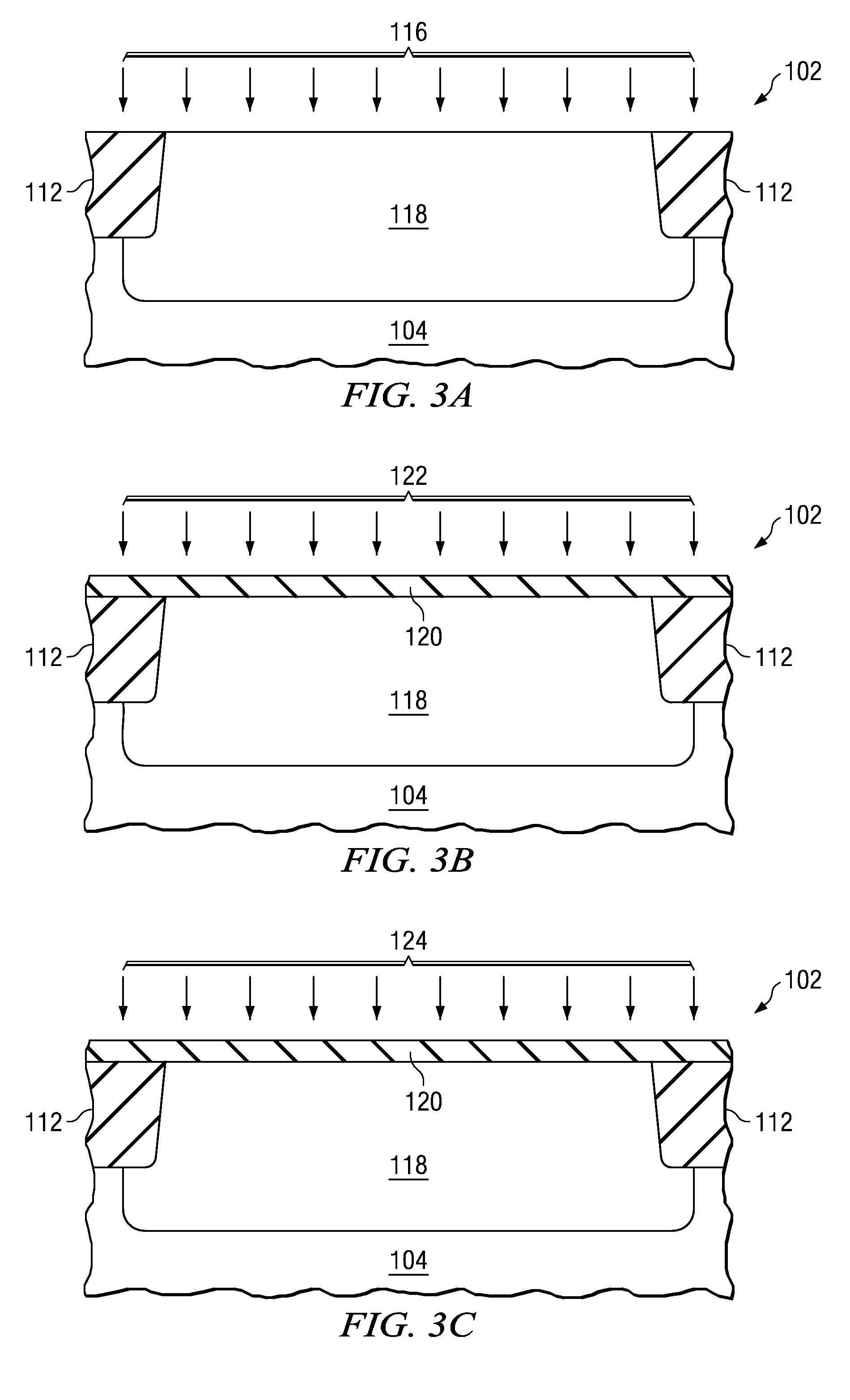
[0018]One or more implementations of the present invention will now be described with reference to the attached drawings, wherein like reference numerals are used to refer to like elements throughout, and wherein the devices and structures illustrated in the figures are not necessarily drawn to scale.

[0019]The invention relates to post-deposition treatment of deposited high-k gate dielectric films to densify the material, heal defects, and to thermally stabilize the material through multiple anneal processes and a nitridation process. The methods of the invention can be employed following high-k deposition and before formation of gate electrode materials over the high-k, to improve the high-k material quality (e.g., reduce point and other defects, densify the material, remove impurities, etc.). The techniques of the invention may be employed in conjunction with any high-k dielectric materials having a dielectric constant “k” greater than that of SiO2 (e.g., greater than about 3.9), ...


PUM

PropertyMeasurementUnit
pressureaaaaaaaaaa
dielectric constantaaaaaaaaaa
temperatureaaaaaaaaaa

Abstract

Methods are disclosed for treating deposited gate dielectric materials, in which the deposited dielectric is subjected to one or more non-oxidizing anneals to densify the material, one or more oxidizing anneals to mitigate material defects, and to a nitridation process to introduce nitrogen into the gate dielectric. The annealing may be performed before and / or after the nitridation to mitigate deposition and / or nitridation defects and to densify the material while mitigating formation of unwanted low dielectric constant oxides at the interface between the gate dielectric and the semiconductor substrate.

Description

RELATED APPLICATIONS[0001]This application is related to U.S. patent application Ser. No. 10 / 185,326, filed on Jun. 28, 2002, entitled ANNEAL SEQUENCE FOR HIGH-K FILM PROPERTY OPTIMIZATION; U.S. patent application Ser. No. 10 / 232,124, filed on Aug. 30, 2002, entitled GATE STRUCTURE AND METHOD; and U.S. Pat. No. 6,544,906, filed Oct. 25, 2001, entitled ANNEALING OF HIGH-K DIELECTRIC MATERIALS, wherein the entirety of these applications and patents are hereby incorporated by reference as if fully set forth herein.FIELD OF INVENTION[0002]The present invention relates generally to semiconductor devices and more particularly to methods for fabricating and treating high dielectric constant gate dielectrics for MOS transistor gate structures.BACKGROUND OF THE INVENTION[0003]Field effect transistors (FETs) are widely used in the electronics industry for switching, amplification, filtering, and other tasks related to both analog and digital electrical signals. Most common among these are met...

Claims


Application Information

Patent Timeline
Patent Type & Authority Patents(United States)
IPC IPC(8): H01L21/336H01L21/28H01L21/314H01L21/316H01L29/51
CPCH01L21/02148H01L21/02271H01L21/02332H01L21/02337H01L21/0234H01L21/28185H01L21/28202H01L21/3144H01L21/3162H01L21/31637H01L21/31641H01L21/31645H01L21/31691H01L29/517H01L29/518
Inventor VISOKAY, MARK R.COLOMBO, LUIGICHAMBERS, JAMES J.ROTONDARO, ANTONIO L. P.BU, HAOWEN
Owner TEXAS INSTR INC
Why Eureka
Try Eureka