Thermal flux laser annealing for ion implantation of semiconductor P-N junctions

Active Publication Date: 2006-11-14
APPLIED MATERIALS INC
View PDF34 Cites 54 Cited by
  • Summary
  • Abstract
  • Description
  • Claims
  • Application Information

AI Technical Summary

Benefits of technology

[0010]A method for forming P—N junctions in a semiconductor wafer includes ion implanting dopant impurities into the wafer and annealing the wafer using a thermal flux laser annealing apparatus that includes an array of semiconductor laser emitters arranged in plural parallel rows extending along a slow axis, plural respective cylindrical lenses overlying respective ones of the rows of laser emitters for collimating light from the respective rows along a fast axis generally perpendicular to the slow axis, a homogenizing light pipe having an input face at a first end for receiving light from the plural cylindrical lenses and an output face at an opposite end, the light pipe comprising a pair of reflecti

Problems solved by technology

The time that the wafer needs to stay at

Method used


Image

  • Thermal flux laser annealing for ion implantation of semiconductor P-N junctions
  • Thermal flux laser annealing for ion implantation of semiconductor P-N junctions
  • Thermal flux laser annealing for ion implantation of semiconductor P-N junctions

Examples


Embodiment Construction

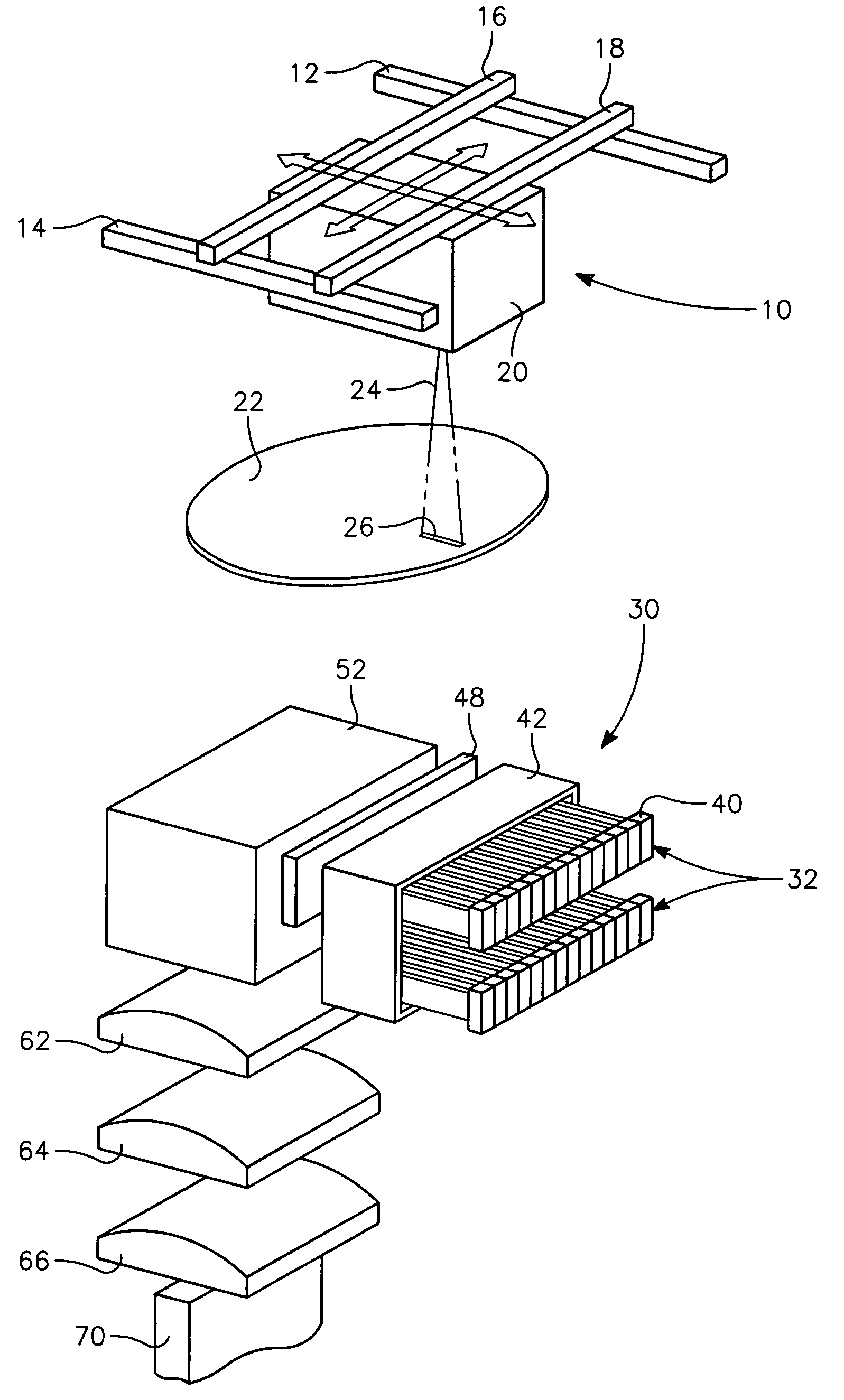
[0023]One embodiment of the apparatus described in the above-referenced application by Jennings et al. is illustrated in the schematic orthographic representation of FIG. 1. A gantry structure 10 for two-dimensional scanning includes a pair of fixed parallel rails 12, 14. Two parallel gantry beams 16, 18 are fixed together a set distance apart and supported on the fixed rails 12, 14 and are controlled by an unillustrated motor and drive mechanism to slide on rollers or ball bearings together along the fixed rails 12, 14. A beam source 20 is slidably supported on the gantry beams 16, 18, and may be suspended below the beams 16, 18 which are controlled by unillustrated motors and drive mechanisms to slide along them. A silicon wafer 22 or other substrate is stationarily supported below the gantry structure 10. The beam source 20 includes a laser light source and optics to produce a downwardly directed fan-shaped beam 24 that strikes the wafer 22 as a line beam 26 extending generally p...


PUM

PropertyMeasurementUnit
Lattice constantaaaaaaaaaa
Semiconductor propertiesaaaaaaaaaa

Abstract

A method for forming P-N junctions in a semiconductor wafer includes ion implanting dopant impurities into the wafer and annealing the wafer using a thermal flux laser annealing apparatus that includes an array of semiconductor laser emitters arranged in plural parallel rows extending along a slow axis, plural respective cylindrical lenses overlying respective ones of the rows of laser emitters for collimating light from the respective rows along a fast axis generally perpendicular to the slow axis, a homogenizing light pipe having an input face at a first end for receiving light from the plural cylindrical lenses and an output face at an opposite end, the light pipe comprising a pair of reflective walls extending between the input and output faces and separated from one another along the direction of the slow axis, and scanning apparatus for scanning light emitted from the homogenizing light pipe across the wafer in a scanning direction parallel to the fast axis.

Description

[0001]This application contains subject matter related to U.S. application Ser. No. 11 / 185,454 filed Jul. 20, 2005 entitled RAPID DETECTION OF IMMINENT FAILURE IN LASER THERMAL PROCESSING OF A SUBSTRATE by Bruce Adams, et al.; U.S. application Ser. No. 11 / 185,649 filed Jul. 20, 2005 entitled SINGLE AXIS LIGHT PIPE FOR HOMOGENIZING SLOW AXIS OF ILLUMINATION SYSTEMS BASED ON LASER DIODES by Bruce Adams, et al.; U.S. application Ser. No. 11 / 195,380 filed Aug. 2, 2005 entitled MULTIPLE BAND PASS FILTERING FOR PYROMETRY IN LASER BASED ANNEALING SYSTEMS by Bruce Adams, et al.; and U.S. application Ser. No. 11 / 198,660 filed Aug. 5, 2005 entitled AUTOFOCUS FOR HIGH POWER LASER DIODE BASED ANNEALING SYSTEM by Dean Jennings, et al., all of which applications are assigned to the present assignee.BACKGROUND OF THE INVENTION[0002]1. Field of the Invention[0003]The invention relates generally to thermal processing of semiconductor substrates. In particular, the invention relates to laser thermal ...

Claims


Application Information

Patent Timeline
IPC IPC(8): H01L21/42
CPCB23K26/0604B23K26/0676B23K26/0738G02B6/4206G02B27/0994H01L21/268H01L21/67115B23K2201/40G02B6/4218H01S5/4012H01S5/405B23K2101/40
Inventor ADAMS, BRUCE E.JENNINGS, DEANMAYUR, ABHILASH J.PARIHAR, VIJAYRANISH, JOSEPH M.
Owner APPLIED MATERIALS INC
Why Eureka
Try Eureka