Layout method of semiconductor integrated circuit, layout structure thereof, and photomask for forming the layout structure

a technology of integrated circuits and layout structures, which is applied in the direction of cad circuit design, originals for photomechanical treatment, instruments, etc., can solve the problems of unintended exposure of resist layers, difficult to achieve processing of device patterns with sufficient precision, and generally extremely difficult to make processing in an area with sufficient precision where patterns have low uniformity, etc., to achieve the effect of eliminating deviation, and reducing the dimensional deviation of resist layers

Active Publication Date: 2006-11-14
KAWASAKI MICROELECTRONICS
View PDF27 Cites 353 Cited by
  • Summary
  • Abstract
  • Description
  • Claims
  • Application Information

AI Technical Summary

Benefits of technology

[0022]It is a further object of this invention to provide a layout method for designing a layout structure of semiconductor integrated circuit in a short period of time with little or no logical synthesizing.
[0088]Thus, exemplary embodiments of this invention provide a method which enables to form a layout structure of a semiconductor integrated circuit on a computer in a short period of time, the layout structure of a semiconductor integrated circuit designed by the layout method, which can be formed on a semiconductor substrate with high dimensional precision, thus eliminating deviation in the pattern dimension and a photomask used for forming a semiconductor integrated circuit having the layout structure on a semiconductor substrate.

Problems solved by technology

In particular, while processing in an area where the patterns having the same dimension are arranged with a uniform density can be made with relative ease, it is generally extremely difficult to make processing in an area with sufficient precision where the patterns have low uniformity.
Accordingly, it is difficult to achieve processing of device patterns with sufficient precision in the outer-most portions of the standard cell array.
However, in reality, some of the exposing light reaches even the area on the semiconductor substrate where the mask pattern is provided, due to scattering of the exposing light passing through the space between the mask patterns.
With the decrease of the pattern dimension, such unintended exposure of the resist layer becomes a significant problem.
However, at the outermost portion of the standard cell array, a greater amount of the unintended exposure occurs because of the scattering of the exposing light that passes through the area outside of the standard cell array, which has a low pattern density.
However, such extensive correction generally leads to a reduction of process margin.
That is, this leads to the problem of the resist pattern becoming susceptible to significant dimensional deviation due to deviation in the exposure light intensity, the deviation of the focus, and so on, over the exposed area.
As a result, the resist pattern formed at the outermost portion of the standard cell array has in general a much poorer precision compared to the inner portion of the standard cell array.
This procedure leads to the creation of a gap between the device pattern and the dummy cell.
In such a layout, while the uniformity of pattern density is improved as compared to a layout having no dummy pattern, the uniformity is not enough to be used in advanced fine patterning technology.
Accordingly, the combination of these conventional technologies presents difficulties in achieving processing with the high precision required for further advanced fine-patterning technology.
Furthermore, a great amount of calculations are required for the logical synthesizing in the technique disclosed in Patent Document 2.
Accordingly, an extremely long time is required for the layout design.

Method used


Image

  • Layout method of semiconductor integrated circuit, layout structure thereof, and photomask for forming the layout structure
  • Layout method of semiconductor integrated circuit, layout structure thereof, and photomask for forming the layout structure
  • Layout method of semiconductor integrated circuit, layout structure thereof, and photomask for forming the layout structure

Examples


Embodiment Construction

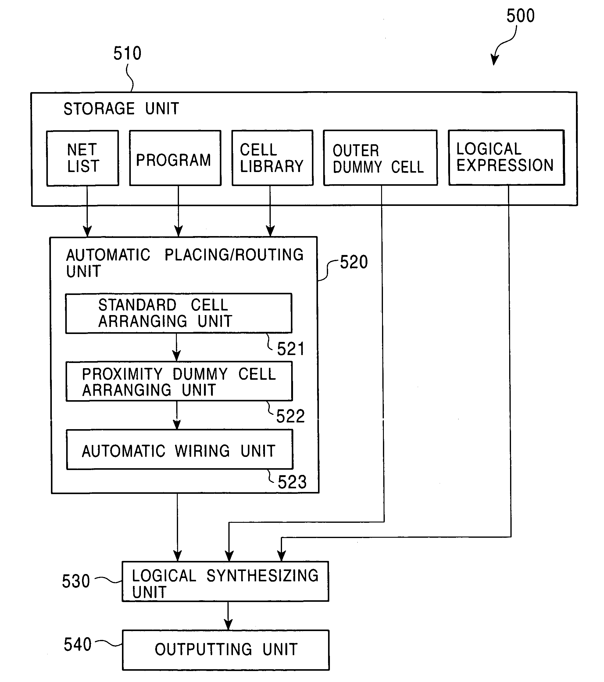
[0117]This invention was first described in Japanese Patent Application No. 2003-297545, which is hereby incorporated by reference in its entirety. Description will be made regarding exemplary embodiments according to this invention with reference to the drawings.

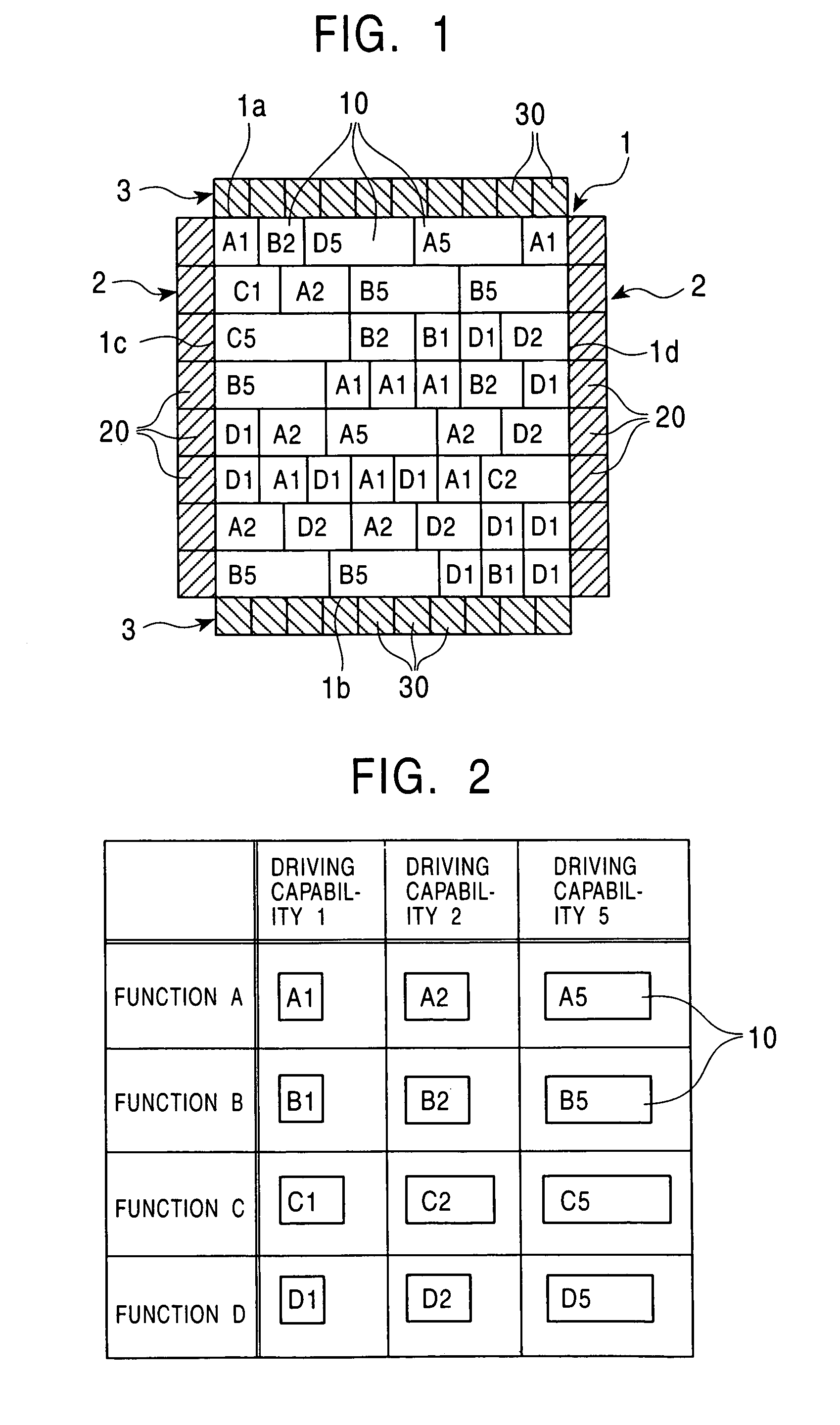
[0118]FIG. 1 is a diagram illustrating an exemplary layout structure of semiconductor integrated circuit according to an exemplary embodiment of this invention.

[0119]FIG. 1 illustrates a layout structure including a standard cell array 1, first proximity dummy bands 2 along the vertical sides of the standard cell array, and second proximity dummy cells 30 along the horizontal sides of the standard cell array. Arranging a plurality of standard cells 10 in rows and columns forms the standard cell array 1. Arranging a plurality of first proximity dummy cells 20 form the first proximity dummy bands 2, and arranging a plurality of second proximity dummy cells 30 forms the second proximity dummy bands 3.

[0120]According to various...


PUM

PropertyMeasurementUnit
widthaaaaaaaaaa
widthaaaaaaaaaa
widthaaaaaaaaaa

Abstract

A plurality of standard cells 10 are arranged to form a channel-less standard cell array 1, which has vertical and horizontal sides. A plurality of first proximity dummy cells 20 are arranged along each of the vertical sides of the standard cell array to form a first proximity dummy bands 20 such that the upper and lower sides of the first proximity dummy cells are in contact with each other and such that the left or right side of each of the first proximity dummy cells is in contact with the vertical side of the standard cell array 1. Furthermore, a plurality of second proximity dummy bands are arranged along each of the horizontal sides of the standard cell array to form a second proximity dummy bands such that the upper or lower side of each of the second proximity dummy cells is in contact with the horizontal side of the standard cell 1.

Description

BACKGROUND OF THE INVENTION[0001]1. Field of Invention[0002]The present invention relates to a layout method of a semiconductor integrated circuit, performed on a computer, a layout structure of a semiconductor integrated circuit designed with the layout method, and a photomask used for manufacturing a semiconductor integrated circuit having the layout structure.[0003]2. Description of Related Art[0004]For designing layouts of semiconductor integrated circuits, standard cell methods have been widely used with the advance of CAD (Computer Aided Design) tools. According to a standard cell method, a plurality of standard cells having circuit patterns for realizing basic logical functions such as an NAND gate, a flip-flop, and the like, are designed, and operations of the standard cells are verified beforehand. Thus, designed and verified standard cells are registered in a library. The user selects specific standard cells for realizing desired logical functions from the library, and arr...

Claims


Application Information

Patent Timeline
Patent Type & Authority Patents(United States)
IPC IPC(8): G06F17/50G03F1/00G03F1/36G03F1/70H01L21/027H01L21/82H01L21/822H01L27/02H01L27/04H01L27/118
CPCG06F17/5068H01L27/0207H01L27/11803G06F30/39
Inventor MAEDA, JUN
Owner KAWASAKI MICROELECTRONICS
Why Eureka
Try Eureka