Method and system for improving usable life of memory devices using vector processing

Active Publication Date: 2006-11-21
ORACLE INT CORP
View PDF10 Cites 83 Cited by
  • Summary
  • Abstract
  • Description
  • Claims
  • Application Information

AI Technical Summary

Benefits of technology

[0014]The present invention is a method, system and apparatus for improving the useful life of non-volatile memory devices such as flash memory. The present wear-leveling technique advantageously improves the overall useful life of a flash memory device by strategically moving inactive logical blocks (logical blocks that have been infrequently modified in the recent past) to the physical blocks that have experienced the most wear (the greatest number of erasures) since the device began operation and by strategically moving active logical blocks to the physical blocks that have experienced the least wear. To track the activity of both

Problems solved by technology

Because non-volatile memory devices are more expensive than volatile memory devices (which lose data when removed from a power source), their use in a computer system is typically limited to situations where a need exists to maintain data even when power is removed or lost.
Certain non-volatile memory devices such as EEPROM age over time, and thus have a limit on the number of times they can be re-programmed.
However, when these devices are used in applications having a large amount of input and output operations—such as when used in conjunction with or in lieu of a disk or tape subsystem—it does become an issue.
The problem is to devise a wear-leveling algorithm that can be relied upon to distribute wear more evenly, with acceptable overheads, under conditions that can be expected to arise in practice.
1. The choice of logical blocks to be moved in a wear-leveling operation

Method used


Image

  • Method and system for improving usable life of memory devices using vector processing
  • Method and system for improving usable life of memory devices using vector processing
  • Method and system for improving usable life of memory devices using vector processing

Examples


Embodiment Construction

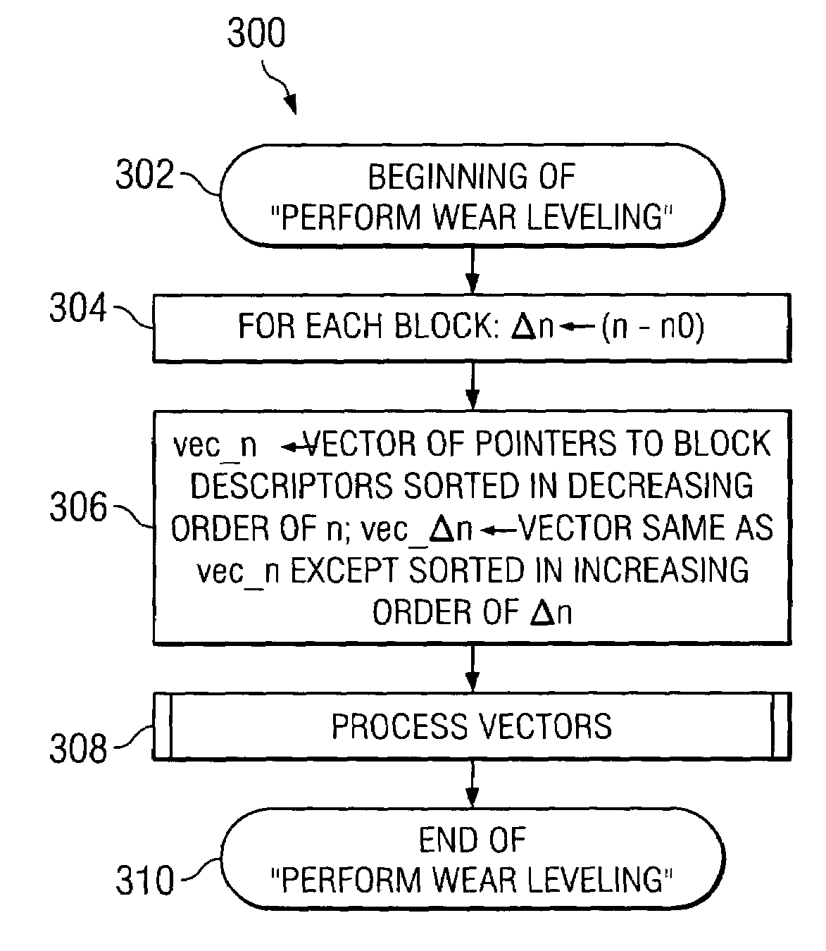
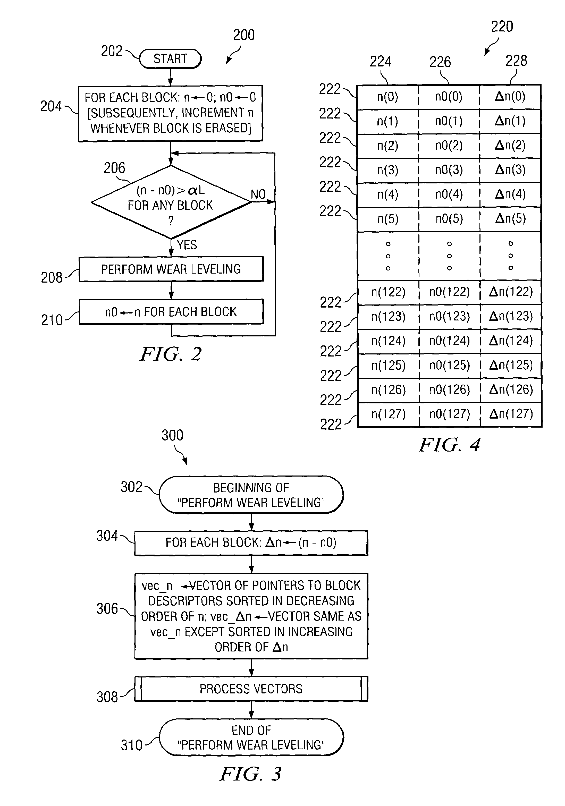
[0027]A technique for leveling the wear of a non-volatile integrated circuit device will increase the life of the device by monitoring storage patterns of the device and relocating certain data to other storage locations based on the activity level of the data and the cumulative wear of the storage locations. The technique works particularly well for EEPROM devices such as flash memory, but the techniques can also be used with other types of non-volatile storage devices such as Ovionics Unified Memory (OUM) and Magnetoresistive RAM (MRAM). As used herein, wear-leveling or a wear-leveling event is the process of moving one or more logical blocks from one physical location to another to more evenly distribute the wear of a non-volatile storage device.

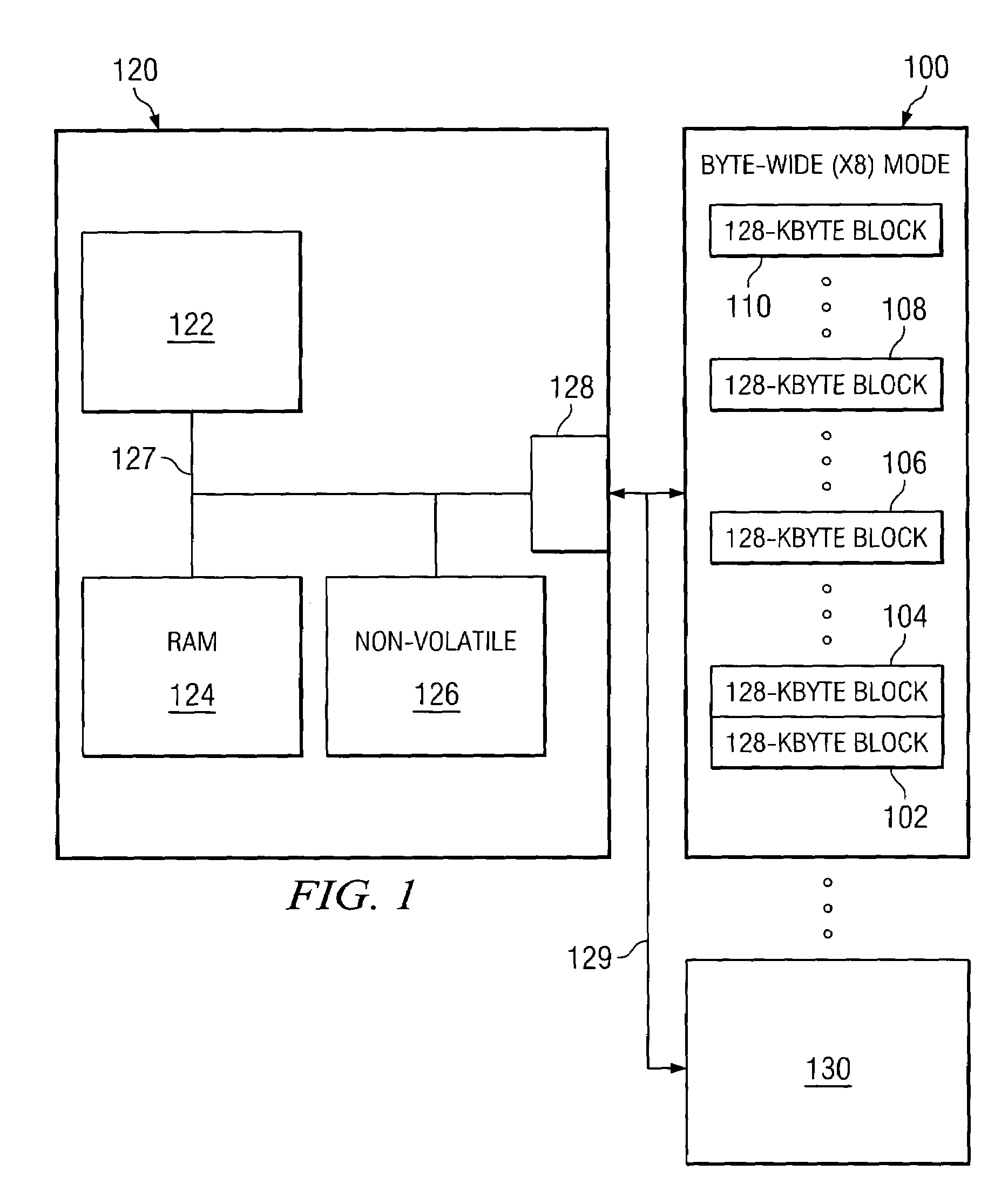
[0028]Flash memory comes in many different sizes such as 64 Mbit, 128 Mbit, 256 Mbit, 512 Mbit and 1 Gbit. Technological advances will soon result in even higher storage densities for flash memory. For purposes of the preferred embodiment...


PUM


Abstract

A method, system and apparatus for improving the useful life of non-volatile memory devices such as flash memory. The present wear-leveling technique advantageously improves the overall useful life of a flash memory device by strategically moving inactive data (data that has been infrequently modified in the recent past) to the memory blocks that have experienced the most wear since the device began operation and by strategically moving active data to the memory blocks that have experienced the least wear. In order to efficiently process and track data activity and block wear, vectors of block-descriptor pointers are maintained. One vector is sorted in decreasing order of overall block erase/write activity (block-wear indicator), whereas the other vector is sorted in increasing order of the number of times a block has been erased since the last wear-leveling event occurred (activity indicator for the data stored in the block). The activity levels of the data and the wear levels of the blocks are then easily compared and otherwise processed using pointers into these vectors to allow for more efficient processing than previous techniques used for wear leveling.

Description

BACKGROUND OF THE INVENTION[0001]1. Field of the Invention[0002]The present invention relates to data storage devices, and in particular relates to improved techniques for using and managing non-volatile memory storage devices to enhance lifetime characteristics of such devices.[0003]2. Background of the Invention[0004]Memory devices are a key component in today's computer systems, allowing high-speed access to retrieve and store data. A certain type of memory device known as non-volatile memory maintains the correct data value stored in the device even when power is removed from the device. Because non-volatile memory devices are more expensive than volatile memory devices (which lose data when removed from a power source), their use in a computer system is typically limited to situations where a need exists to maintain data even when power is removed or lost. For example, configuration settings for a computer are typically stored in non-volatile memory so that the system properly ...

Claims


Application Information

Patent Timeline
IPC IPC(8): G06F12/00
CPCG06F12/0246G06F2212/1036G06F2212/7211
Inventor DEFOUW, RICHARD JOHNNGUYEN, THAI
Owner ORACLE INT CORP
Why Eureka
Try Eureka