Electron beam lithography method using new material

a lithography method and eb technology, applied in photomechanical equipment, instruments, nuclear engineering, etc., can solve the problems of reaching the technical limit of forming finer patterns, difficult to reduce the linewidth of patterns to a sufficient degree, etc., and achieve the effect of further reducing the linewidth of patterns

Inactive Publication Date: 2006-12-05
SAMSUNG ELECTRONICS CO LTD
View PDF2 Cites 20 Cited by
  • Summary
  • Abstract
  • Description
  • Claims
  • Application Information

AI Technical Summary

Benefits of technology

[0007]The present invention may provide an electron beam (EB) lithography method using a new material, which can further reduce the linewidth of patterns as compared to conventional methods.
[0025]According to the EB lithography method of the present invention, a thin layer formed of a Pb-based material is patterned using e-beams, so that the linewidth of patterns can be further reduced.

Problems solved by technology

For example, in a UV-photolithography process as a conventional fine processing technique, since the resolution and comformability of patterns are limited to 1 μm and ±3 μm, respectively, it becomes difficult to reduce the linewidth of the patterns to a sufficient degree.
However, the conventional EB lithography technique is reaching the technical limit for forming finer patterns.

Method used


Image

  • Electron beam lithography method using new material
  • Electron beam lithography method using new material
  • Electron beam lithography method using new material

Examples


Embodiment Construction

[0031]The present invention will now be described more fully hereinafter with reference to the accompanying drawings, in which exemplary embodiments of the invention are shown. In the drawings, the same reference numerals are used to denote the same elements, and the thicknesses of layers and regions are exaggerated for clarity.

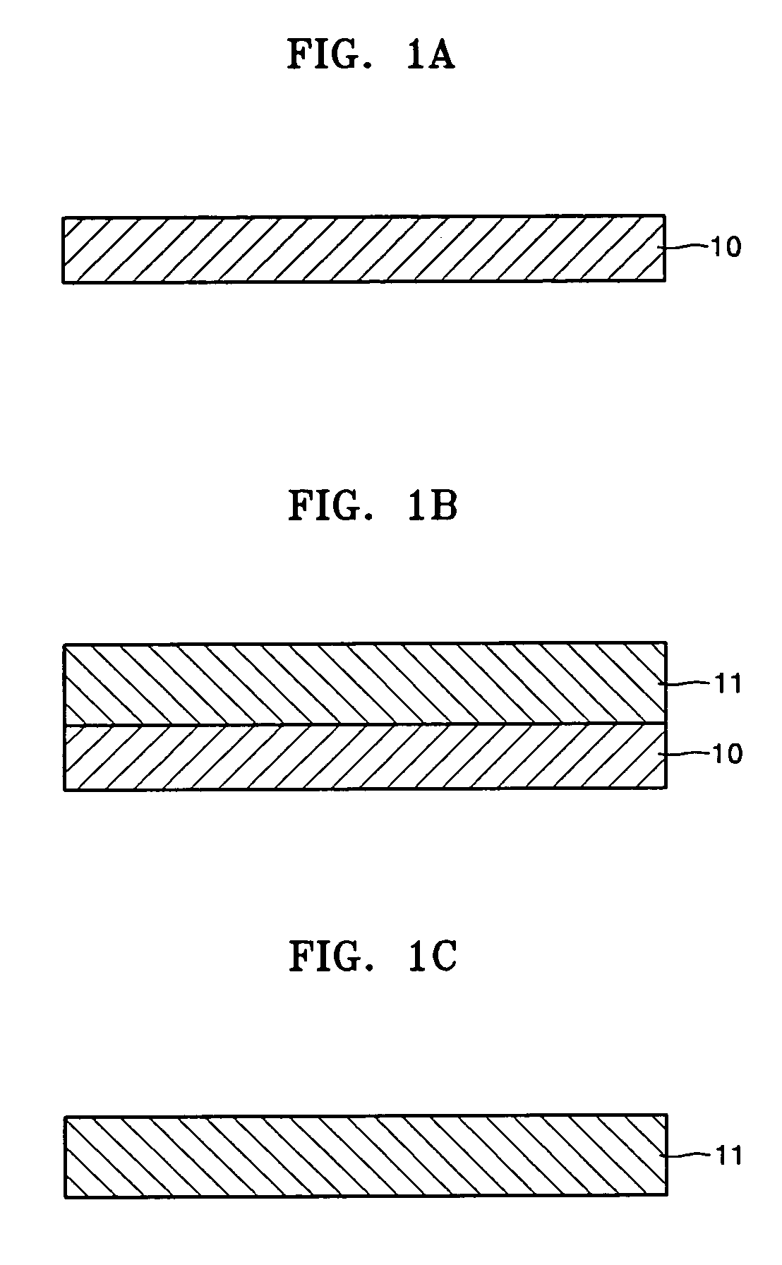
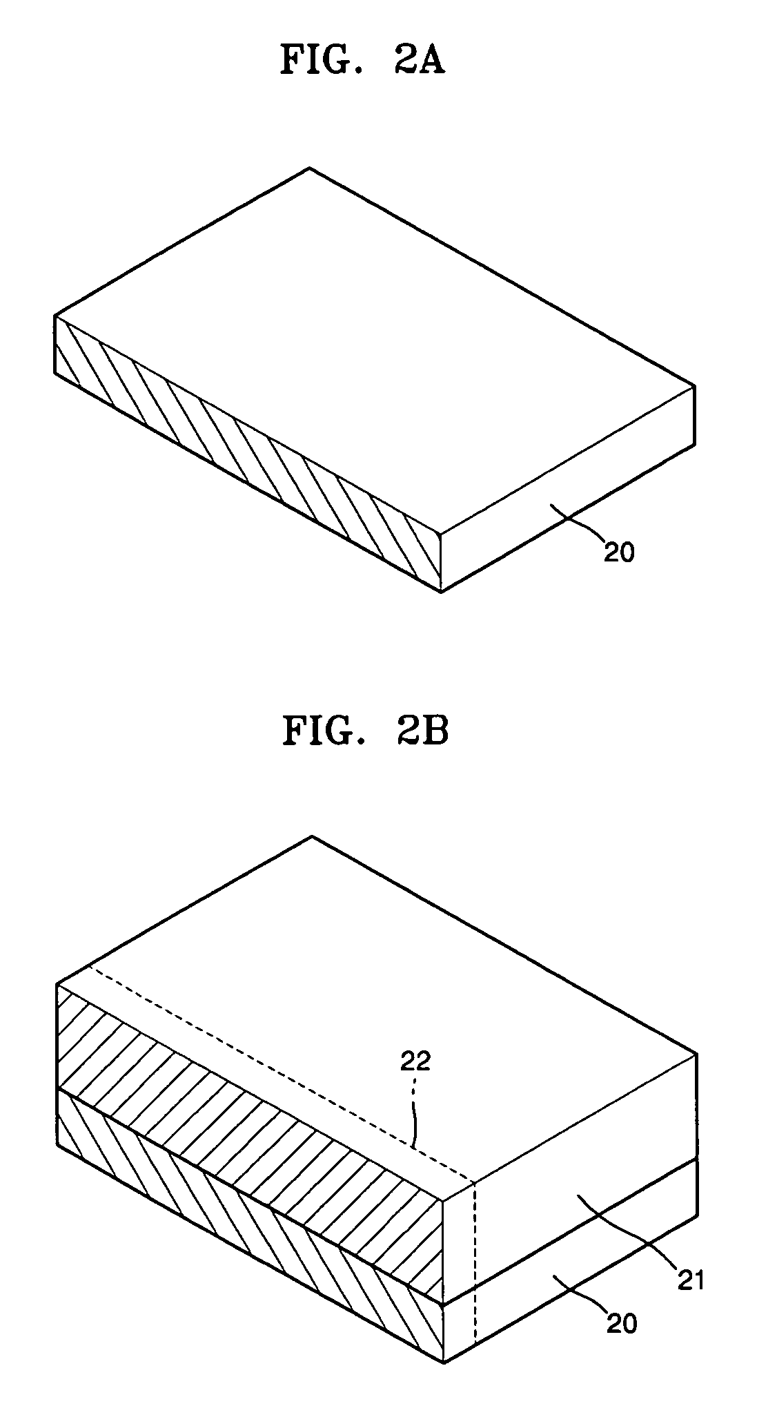
[0032]FIGS. 1A through 1C are cross-sectional views illustrating an electron beam (EB) lithography method according to an exemplary embodiment of the present invention.

[0033]Referring to FIG. 1A, a substrate 10 is prepared. In the present embodiment, the substrate 10 is removed before a patterning process is performed on a thin layer. Thus, the substrate 10 may be formed of a material that is easily removed using a physical or chemical technique. In the present embodiment, the substrate 10 may be formed of polycarbonate that is soluble in a chloroform solution. In another case, the substrate 10 may be formed of water-soluble sodium chloride (NaCl).

[0034]There...


PUM

PropertyMeasurementUnit
thicknessaaaaaaaaaa
thicknessaaaaaaaaaa
acceleration voltageaaaaaaaaaa

Abstract

An electron beam (EB) lithography method using a new material is provided. The method includes forming a thin layer using a Pb-based material; and patterning the thin layer by partially volatilizing the thin layer by irradiating electron beams. In this method, the thin layer formed of the Pb-based material is patterned using e-beams so that the linewidth of patterns formed on the thin layer can be greatly reduced.

Description

CROSS-REFERENCE TO RELATED PATENT APPLICATION[0001]This application claims the benefit of Korean Patent Application No. 10-2004-0112299, filed on Dec. 24, 2004, in the Korean Intellectual Property Office, the disclosure of which is incorporated herein in its entirety by reference.BACKGROUND OF THE DISCLOSURE[0002]1. Field of the Invention[0003]The disclosure relates to an electron beam (EB) lithography method, more particularly, to an EB lithography method using a new material.[0004]2. Description of the Related Art[0005]An electron beam (EB) lithography process is used to delineate a circuit pattern during the fabrication of a semiconductor integrated circuit (IC). In general, a lithography process includes transferring a mask pattern onto a photoresist; and etching an underlying layer using a pattern of the transferred photoresist. The process of transferring the mask pattern has primarily been performed using light (especially ultraviolet (UV) rays). However, as the integration d...

Claims


Application Information

Patent Timeline
Patent Type & Authority Patents(United States)
IPC IPC(8): G03C5/00
CPCB82Y10/00B82Y40/00G03F7/0043G03F7/167H01J37/3174G03F7/2051H01J2237/3174H01J2237/31754H01J2237/31796Y10S430/143G03F7/70383G03C5/00
Inventor PARK, JONG-BONGCHOI, CHEL-JONG
Owner SAMSUNG ELECTRONICS CO LTD
Why Eureka
Try Eureka