

He treatment to improve low-k adhesion property
a low-k adhesion and film technology, applied in the manufacturing of basic electric elements, semiconductor/solid-state devices, electric apparatus, etc., can solve the problems of poor adhesion and reliability concerns, and achieve the effects of improving the adhesion of low-k dielectric films
- Summary
- Abstract
- Description
- Claims
- Application Information
AI Technical Summary
Benefits of technology
Problems solved by technology
Method used
Image


Examples
Embodiment Construction
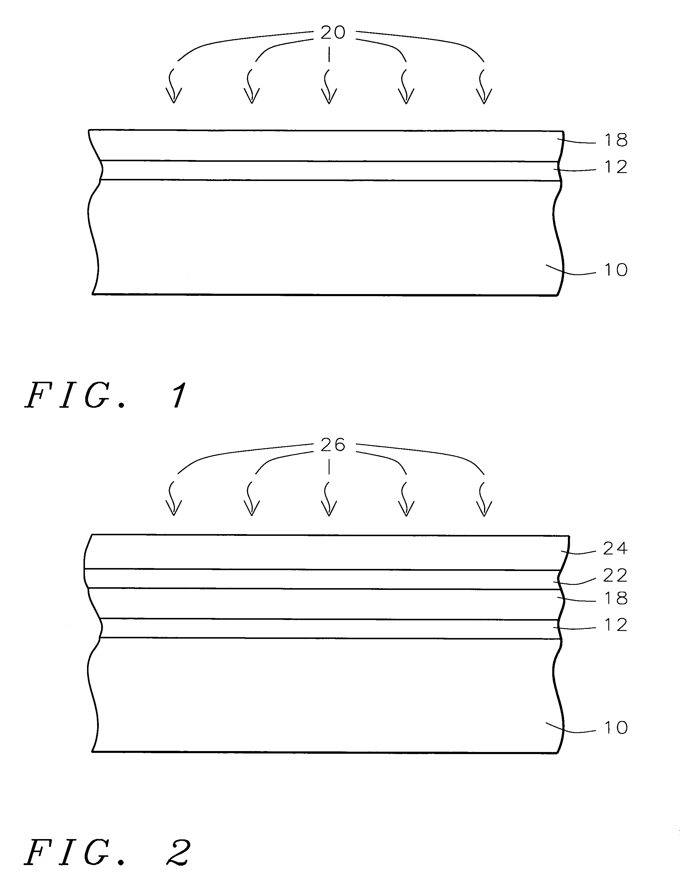
[0012]The present invention proposes a method of improving adhesion of low dielectric constant films to other dielectric films. It will be understood by those skilled in the art that the present invention should not be limited to the application illustrated in the drawings, but can be extended and applied to any application in which improved adhesion of dielectric films to overlying layers is desired.
[0013]Referring now more particularly to FIG. 1, there is illustrated a portion of a partially completed integrated circuit device. There is shown a substrate 10, preferably composed of monocrystalline silicon. Device structures, such as gate electrodes, source and drain regions, and metal interconnects, not shown, are formed in and on the substrate and covered with an insulating layer. A passivation or barrier layer 12 may be formed over the device structures to a thickness of between about 250 and 600 Angstroms. For example, a silicon carbide layer may be used.
[0014]A first low dielec...
PUM
| Property | Measurement | Unit |
|---|---|---|
| pressure | aaaaa | aaaaa |
| pressure | aaaaa | aaaaa |
| temperature | aaaaa | aaaaa |
Abstract
Description
Claims
Application Information