Chip interconnect and packaging deposition methods and structures

a technology of interconnects and packaging, applied in the direction of superimposed coating process, liquid/solution decomposition chemical coating, coating, etc., can solve the problems of high cost of conventional cmp process, large number of defects on substrates, and long polishing time, so as to achieve efficient and time-saving manner

Inactive Publication Date: 2006-12-12
NOVELLUS SYSTEMS
View PDF31 Cites 419 Cited by
  • Summary
  • Abstract
  • Description
  • Claims
  • Application Information

AI Technical Summary

Benefits of technology

[0017]It is an object of the present invention to provide a method that removes the seed layer from a top surface of a substrate while preventing or minimizing removal of the seed layer from the cavities of the substrate.
[0019]It is a further object of the present invention to provide a method that removes a seed layer from a top surface of a substrate using a pad type material while preventing removal of the seed layer from the cavities of the substrate.
[0020]It is yet another object of the present invention to provide a method that removes the seed layer from a top surface of a substrate while depositing a conductive material in the cavities of the substrate.
[0021]It is another object of the present invention to provide a method that reduces and minimizes the conductive material overburden across a substrate while depositing the conductive material in the cavities of the substrate.
[0022]It is yet another object of the present invention to provide a method that minimizes the disparity of the conductive material overburden across a substrate while depositing the conductive material in the cavities of the substrate.
[0025]The present invention discloses methods for depositing a conductive material in cavities of a substrate in a more efficient and time saving manner. One method according to the present invention includes selectively removing portions of a seed layer from a top surface of a substrate and then depositing a conductive material in the cavities of the substrate, where portions of the seed layer remains in the cavities. A pad type material that is attached to an anode is used to polish the seed layer from the top surface of the substrate. Another method includes forming an oxide layer on the top surface of the substrate such that the conductive material can be deposited in the cavities without the material being formed on the top surface of the substrate. The present invention also discloses the structures that are formed using the methods described herein.

Problems solved by technology

The disparity of the conductive material 8 overburden across the substrate results in longer polishing time and higher costs using the conventional CMP process.
In this case, applying the photoresist material on the discontinuous seed layer in the cavities may result in portions of the seed layer being consumed by the photoresist material, thereby resulting in a substrate having a large number of defects.
When the abrasives are attached to the sidewalls of the cavities, they are often very difficult to remove, thereby resulting in substrates have various defects when the conductive material is deposited in the cavities.

Method used


Image

  • Chip interconnect and packaging deposition methods and structures
  • Chip interconnect and packaging deposition methods and structures
  • Chip interconnect and packaging deposition methods and structures

Examples


Embodiment Construction

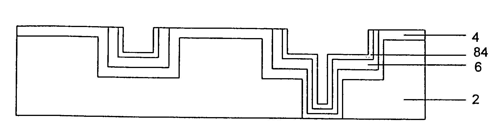
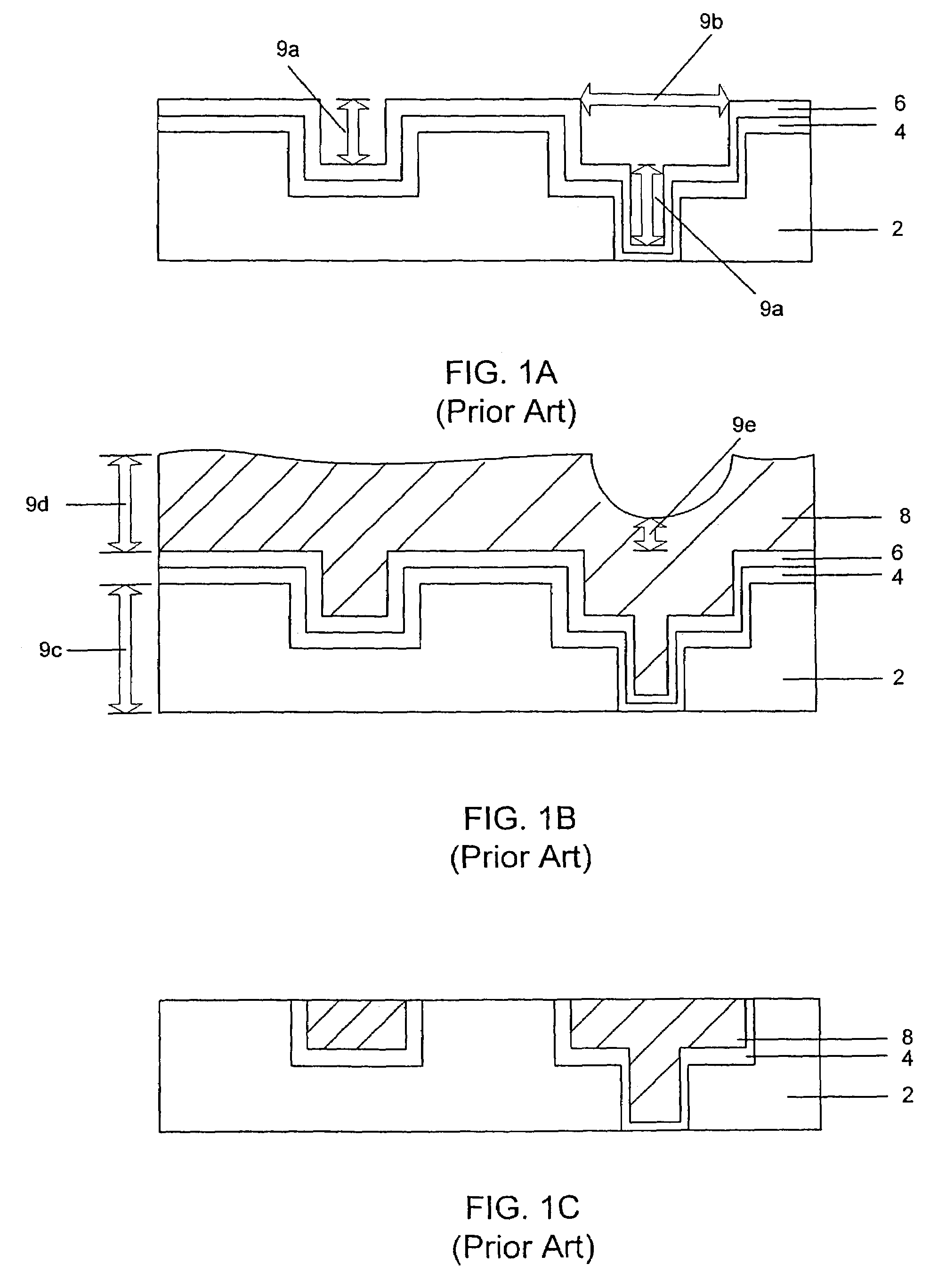
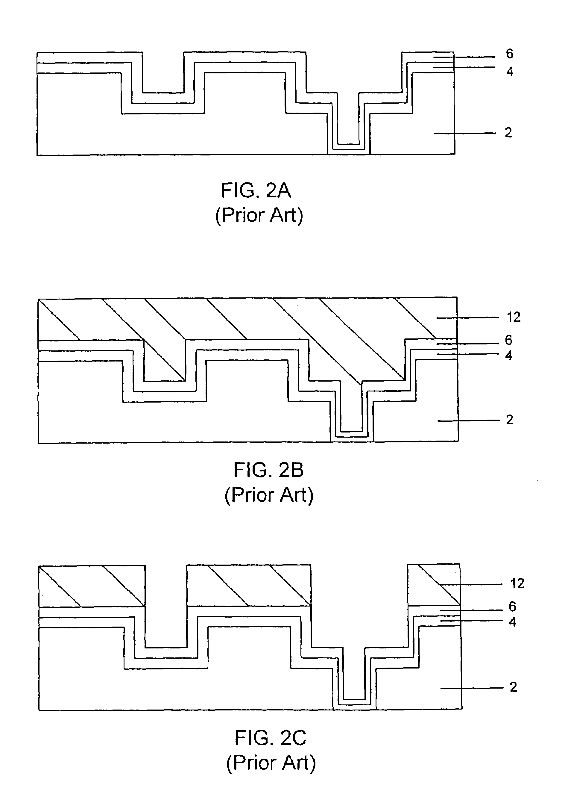
[0035]The preferred embodiments of the present invention will now be described with reference to FIGS. 3–8, wherein like structures and materials are designated by like reference numerals throughout the various figures. The inventors of the present invention disclose herein methods for depositing a conductive material, preferably copper, in cavities of a substrate. The present invention can be used with any substrate or workpiece such as a wafer, flat panel, magnetic film head, integrated circuit, device, chip, and packaging substrate including lead-tin solder alloys, or lead free solderable alloys. Further, specific processing parameters provided herein are intended to be explanatory rather than limiting.

[0036]FIGS. 3A–3D illustrate cross sectional views of methods for fabricating chip interconnects and packages in accordance with the present invention. In other words, FIGS. 3A–3D disclose methods for depositing a material, preferably a conductive material / solution such as copper, ...


PUM

PropertyMeasurementUnit
depthaaaaaaaaaa
widthaaaaaaaaaa
widthaaaaaaaaaa

Abstract

The present invention relates to a method for fabricating high performance chip interconnects and packages by providing methods for depositing a conductive material in cavities of a substrate in a more efficient and time saving manner. This is accomplished by selectively removing portions of a seed layer from a top surface of a substrate and then depositing a conductive material in the cavities of the substrate, where portions of the seed layer remains in the cavities. Another method includes forming an oxide layer on the top surface of the substrate such that the conductive material can be deposited in the cavities without the material being formed on the top surface of the substrate. The present invention also discloses methods for forming multi-level interconnects and the corresponding structures.

Description

REFERENCE TO RELATED APPLICATIONS[0001]This application is a continuation of Ser. No. 09 / 905,335 filed Jul. 13, 2001(NT-013DIV) now U.S. Pat. No. 6,905,588, which is a divisional of Ser. No. 09 / 398,258 filed Sep. 17, 1999, now U.S. Pat. No. 6,355,153 (NT-013), all incorporated herein by reference.FIELD OF THE INVENTION[0002]The present invention relates to a method for fabricating high performance chip interconnects and packages. More particularly, the present invention is directed to a method for insitu-selectively removing portions of a seed layer from a top surface of a substrate while preventing removal of the seed layer from the cavities formed therein. Moreover, the present invention discloses methods for depositing a conductive material in cavities of a substrate.BACKGROUND OF THE INVENTION[0003]Depositing a metal / conductive material in cavities (trenches, holes, and vias) of a substrate or workpiece has important and broad application in the semiconductor and non-semiconduct...

Claims


Application Information

Patent Timeline
Patent Type & Authority Patents(United States)
IPC IPC(8): C25D5/02C25D5/48C25D5/52C25D3/02C23C28/00C25D5/10C25D7/12H01L21/288H01L21/304H01L21/60H01L21/768
CPCC25D5/02C25D5/10C25D5/22C25D5/34H01L21/2885H01L21/7684H01L21/76843H01L21/76855H01L21/76865H01L21/76871H01L21/76874H01L21/76876H01L21/76879H01L21/76885H01L24/11C23C18/1848C23C18/1608C23C18/31H01L2221/1089H01L2224/13099H01L2924/01002H01L2924/01013H01L2924/01015H01L2924/01016H01L2924/01022H01L2924/01027H01L2924/01029H01L2924/0103H01L2924/01033H01L2924/01042H01L2924/01046H01L2924/01047H01L2924/01049H01L2924/01057H01L2924/0106H01L2924/01073H01L2924/01074H01L2924/01078H01L2924/01079H01L2924/01082H01L2924/04941H01L2924/04953H01L2924/14H01L2924/3011H01L2924/01006H01L2924/01019H01L2924/01021H01L2924/01024H01L2924/01041H01L2924/01044H01L2924/01045H01L2924/01072H01L2924/01087H01L2924/014C23C18/1696C23C18/165C23C18/1651C23C18/1653H01L21/283
Inventor UZOH, CYPRIAN EMEKATALIEH, HOMAYOUNBASOL, BULENT
Owner NOVELLUS SYSTEMS
Why Eureka
Try Eureka