

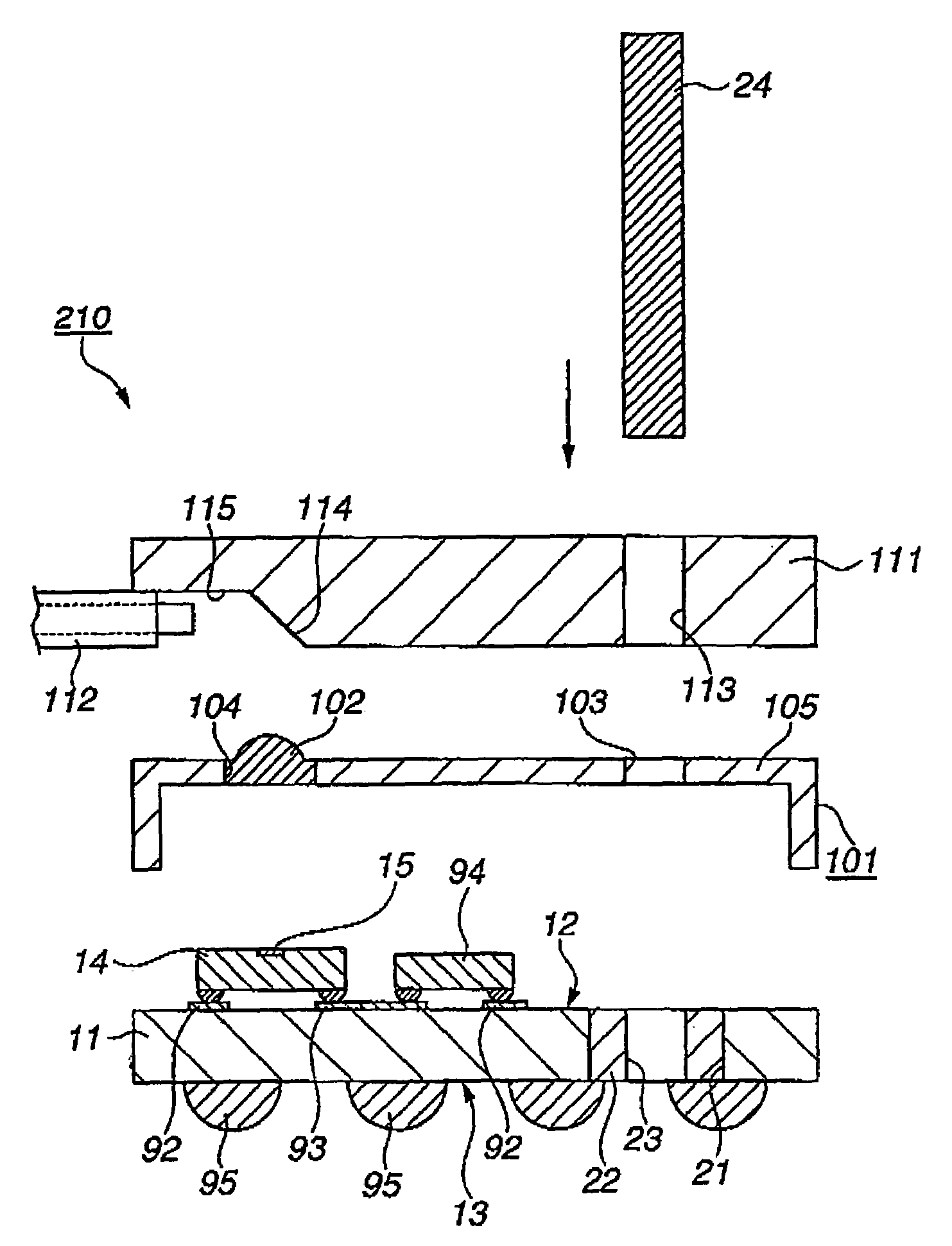
Optical device mounted substrate assembly
a technology of optical devices and substrates, applied in the direction of optical elements, instruments, optical waveguide light guides, etc., can solve the problems of insufficient alignment accuracy, optical transmission loss, and techniques considered incapable of meeting the demand for high speed and high density optical communication, and achieve the effect of improving the accuracy of optical axis alignmen
- Summary
- Abstract
- Description
- Claims
- Application Information
AI Technical Summary
Benefits of technology
Problems solved by technology
Method used
Image

Examples
modified example
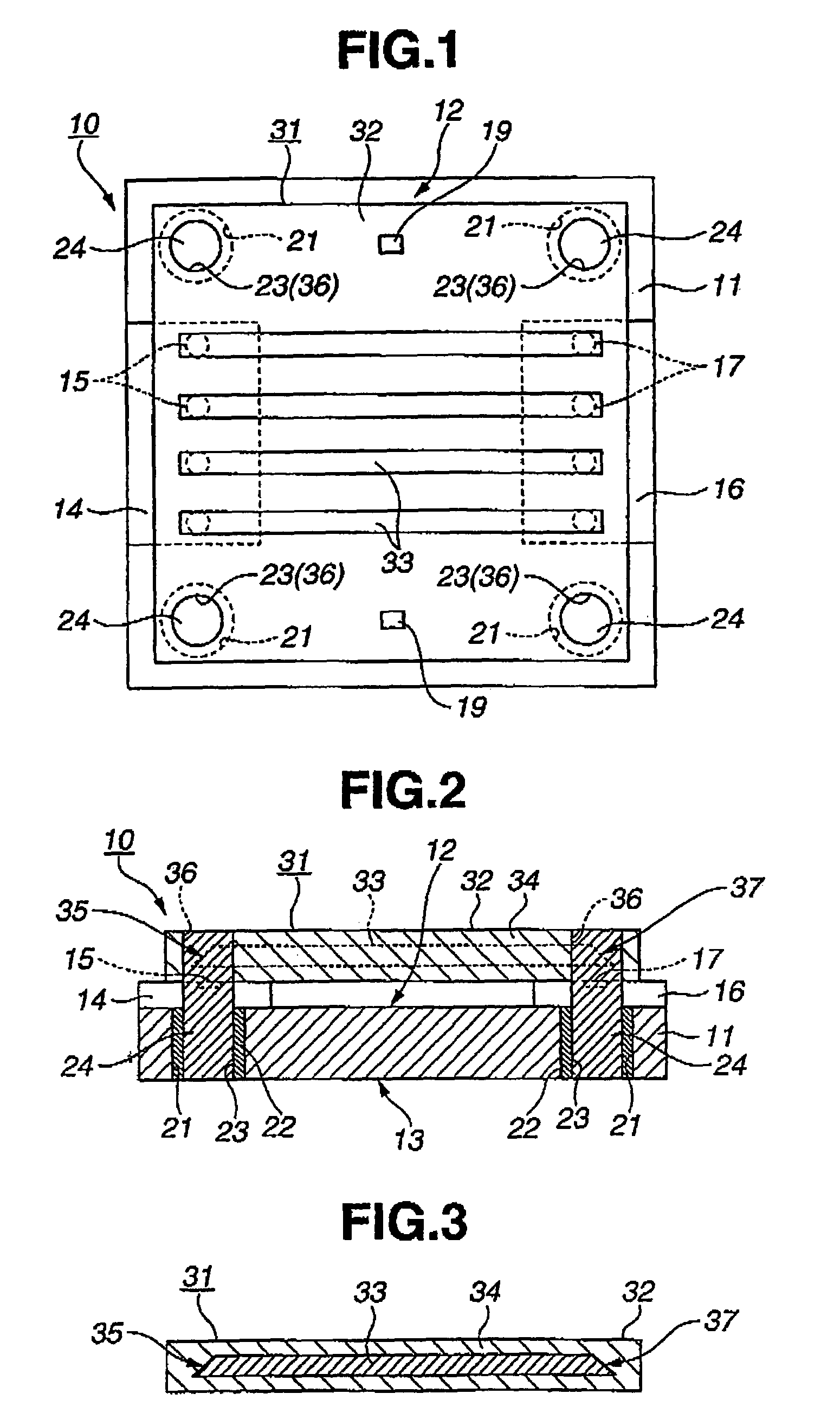
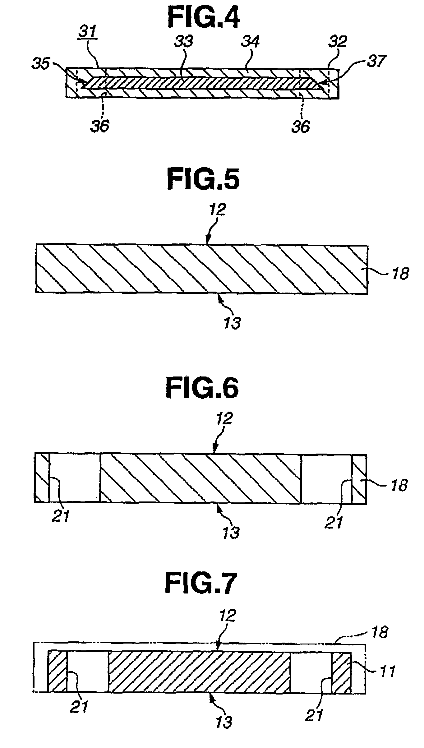
[0170]FIGS. 30 and 31 depict a modified example of the optical waveguide equipped optical device mounted substrate assembly (substrate assembly for supporting an optical component equipped with another optical component) 510 according to the sixth embodiment of the present invention. FIG. 30 is a schematic cross-sectional view illustrating an optical waveguide equipped optical device mounted substrate assembly 510 of the modified example. FIG. 31 is a cross-sectional view taken along line 31—31 of FIG. 30.
[0171]In the optical waveguide equipped optical device mounted substrate assembly 510, the wiring layers (the connecting pads 92 and the metal interconnect layer 93) of the under side optical waveguide 141 are omitted, and instead, connecting pads 158 are disposed on the bottom surface of a cavity 136. A VCSEL 14 and an active circuit IC 94 are soldered on the connecting pads 158. Furthermore, each of cores 33 of an upper side optical waveguide 151 and each of cores 33 of an under ...
PUM
| Property | Measurement | Unit |
|---|---|---|
| diameter | aaaaa | aaaaa |
| diameter | aaaaa | aaaaa |
| diameter | aaaaa | aaaaa |
Abstract
Description
Claims
Application Information