Determination of device failure characteristic

a technology of failure characteristic and device, which is applied in the direction of instrumentation, semiconductor operation lifetime testing, testing circuits, etc., can solve the problems of limited qualification of other characteristics of mosfet, the expected life-time of the semiconductor device,

Inactive Publication Date: 2006-12-26
ADVANCED MICRO DEVICES INC
View PDF3 Cites 16 Cited by
  • Summary
  • Abstract
  • Description
  • Claims
  • Application Information

AI Technical Summary

Problems solved by technology

The failure characteristic typically includes an expected life-time of the semiconductor device.
However, the TDDB method uses capacitor structures for characterizing the quality of the gate dielectric of a MOSFET and is limited in qualifying other characteristics of the MOSFET.

Method used


Image

  • Determination of device failure characteristic
  • Determination of device failure characteristic
  • Determination of device failure characteristic

Examples


Embodiment Construction

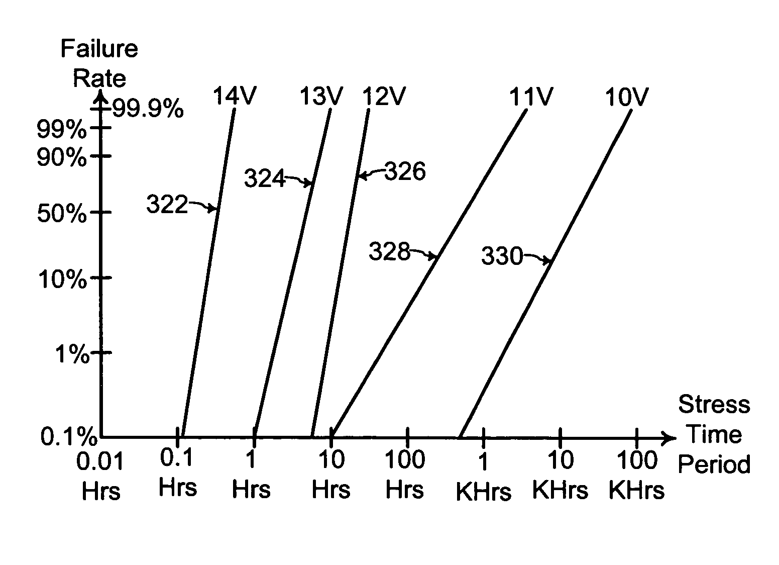
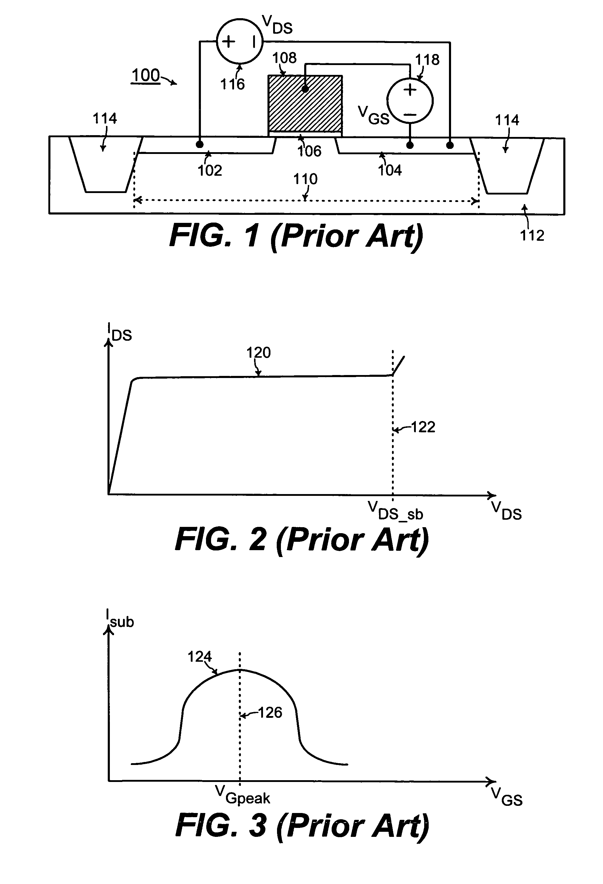
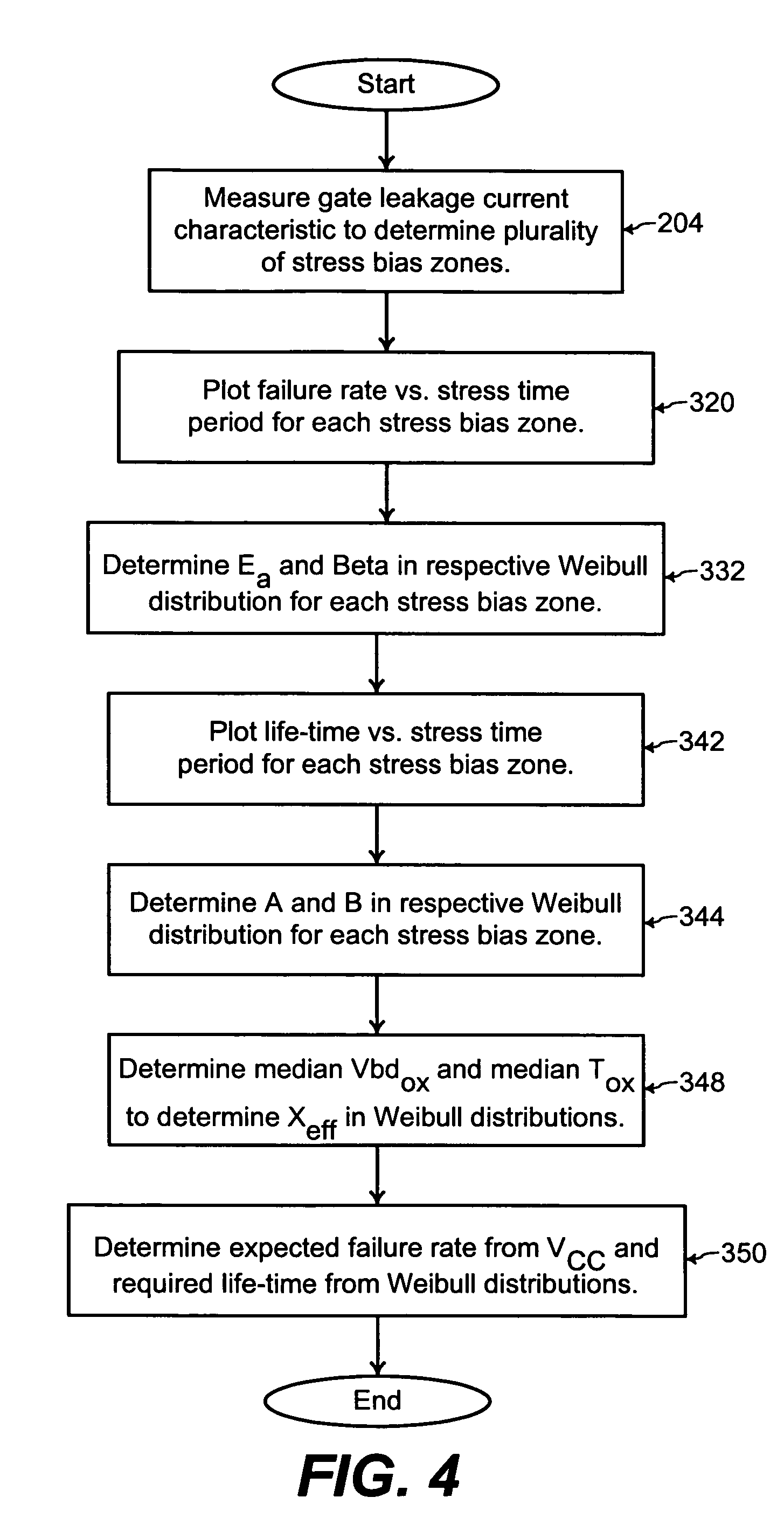
[0035]FIG. 4 shows a flowchart with steps for determining a respective failure characteristic of test MOSFETs (metal oxide semiconductor field effect transistors) such as a test MOSFET 200 of FIG. 5 for a plurality of stress bias zones, according to an embodiment of the present invention. First, a gate leakage current characteristic 202 as illustrated in FIG. 6 is measured (step 204 of FIG. 4).

[0036]Referring to FIG. 5, the MOSFET 200 includes a drain 206, a source 208, a gate dielectric 210, and a gate structure 212 formed within an active device area 214 of the semiconductor substrate 216. The active device area 214 is surrounded by STI (shallow trench isolation) structures 218. For measuring the gate leakage current characteristic 202, a variable gate bias voltage source 220 and a current meter 222 are coupled in series between the gate structure 212 and the source 208 of the MOSFET 200. In addition, the drain 206, the source 208, and the substrate 216 are coupled to ground.

[0037...


PUM


Abstract

For determining a failure characteristic of a semiconductor device, a leakage current characteristic is measured for the semiconductor device to determine a plurality of stress bias zones. A respective set of parameters that define a respective failure characteristic of the semiconductor device is determined for each of the stress bias zones such that the failure characteristic is accurately determined for a wide range of operating voltages.

Description

TECHNICAL FIELD[0001]The present invention relates generally to integrated circuit fabrication, and more particularly, to accurately determining the failure characteristic of a semiconductor device such as a MOSFET (metal oxide semiconductor field effect transistor).BACKGROUND OF THE INVENTION[0002]The failure characteristic of a semiconductor device is an important specification for customers of the semiconductor device. The failure characteristic typically includes an expected life-time of the semiconductor device. For determining such a failure characteristic, the semiconductor device is stressed with application of stress bias voltages.[0003]FIG. 1 shows a MOSFET (metal oxide semiconductor field effect transistor) 100 as the semiconductor device that is a common component of integrated circuits. The MOSFET 100 includes a drain 102, a source 104, a gate dielectric 106, and a gate structure 108 formed within an active device area 110 of the semiconductor substrate 112. The active ...

Claims


Application Information

Patent Timeline
Patent Type & Authority Patents(United States)
IPC IPC(8): G06F15/00
CPCG01R31/2621G01R31/2642G01R31/287
Inventor KIM, HYEON-SEAGMARATHE, AMITTAYLOR, KURT
Owner ADVANCED MICRO DEVICES INC
Why Eureka
Try Eureka