Magnetic memory device and method of manufacturing magnetic memory device

a magnetic memory and memory device technology, applied in the direction of solid-state devices, transistors, instruments, etc., can solve the problems of complex structure and achieve the effect of stably writing and efficiently manufacturing

Inactive Publication Date: 2007-01-02
TDK CORPARATION
View PDF11 Cites 2 Cited by
  • Summary
  • Abstract
  • Description
  • Claims
  • Application Information

AI Technical Summary

Benefits of technology

[0011]The present invention has been achieved in consideration of such problems and its object is to provide a magnetic memory device to which information can be stably written by efficiently using a magnetic field generated by current flowing in a conductor and which can be manufactured more easily and a method of manufacturing the same.
[0019]Since the methods of manufacturing a magnetic memory device according to the first and second aspect of the invention include the step of simultaneously forming the pair of first write lines and the pair of second write lines so as to be disposed adjacent to each other in the first level, as compared with the case of separately forming the first and second write lines, the number of processes is reduced.
[0022]Since the method of manufacturing a magnetic memory device according to the invention includes the third step of simultaneously forming the first and second write lines so as to be disposed adjacent to each other in the first level via the first insulating film over the lower yoke, the first and second write lines can be formed simultaneously in the region surrounded by the magnetic yoke. Thus, the manufacturing process can be simplified.

Problems solved by technology

However, in the magnetic memory device including the magnetic memory cell having the closed magnetic circuit structure as disclosed in Japanese Patent Laid-open No. 2001-273759, the structure is more complicated as compared with a magnetic memory device which does not have the closed magnetic circuit structure.

Method used


Image

  • Magnetic memory device and method of manufacturing magnetic memory device
  • Magnetic memory device and method of manufacturing magnetic memory device
  • Magnetic memory device and method of manufacturing magnetic memory device

Examples


Embodiment Construction

[0051]Embodiments of the invention will now be described in detail hereinbelow by referring to the drawings.

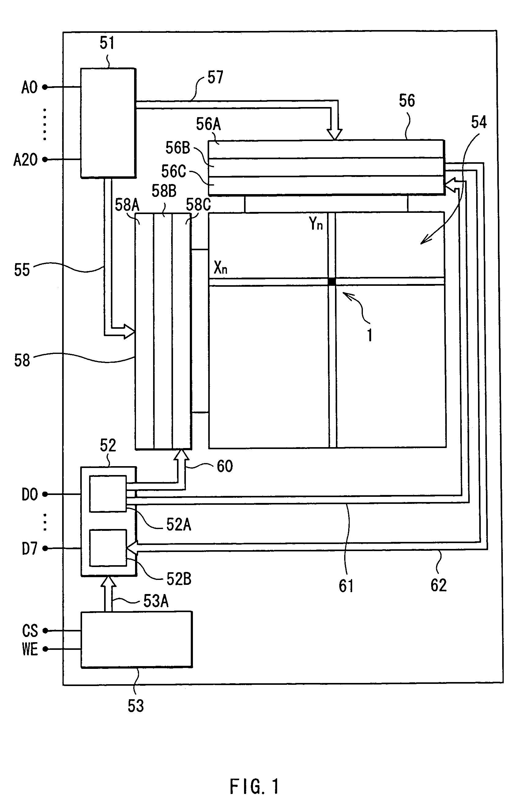
[0052]First, by referring to FIGS. 1 to 9, the configuration of a magnetic memory device according to an embodiment of the invention will be described. FIG. 1 is a conceptual diagram showing a general configuration of a magnetic memory device in the embodiment. The magnetic memory device has an address buffer 51, a data buffer 52, a control logic part 53, a memory cell group 54, a first drive control circuit part 56, a second drive control circuit part 58, external address input terminals A0 to A20, and external data terminals D0 to D7.

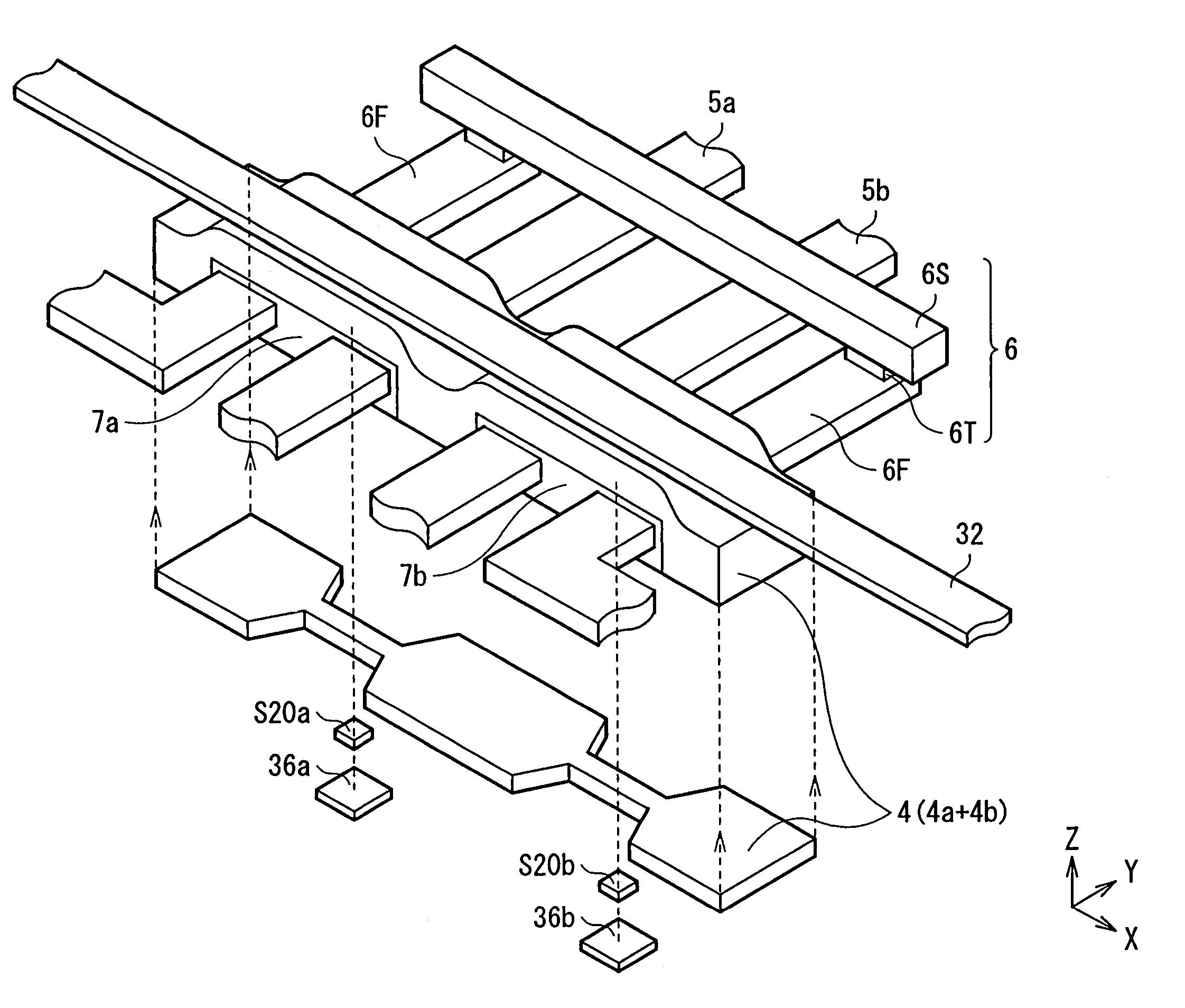
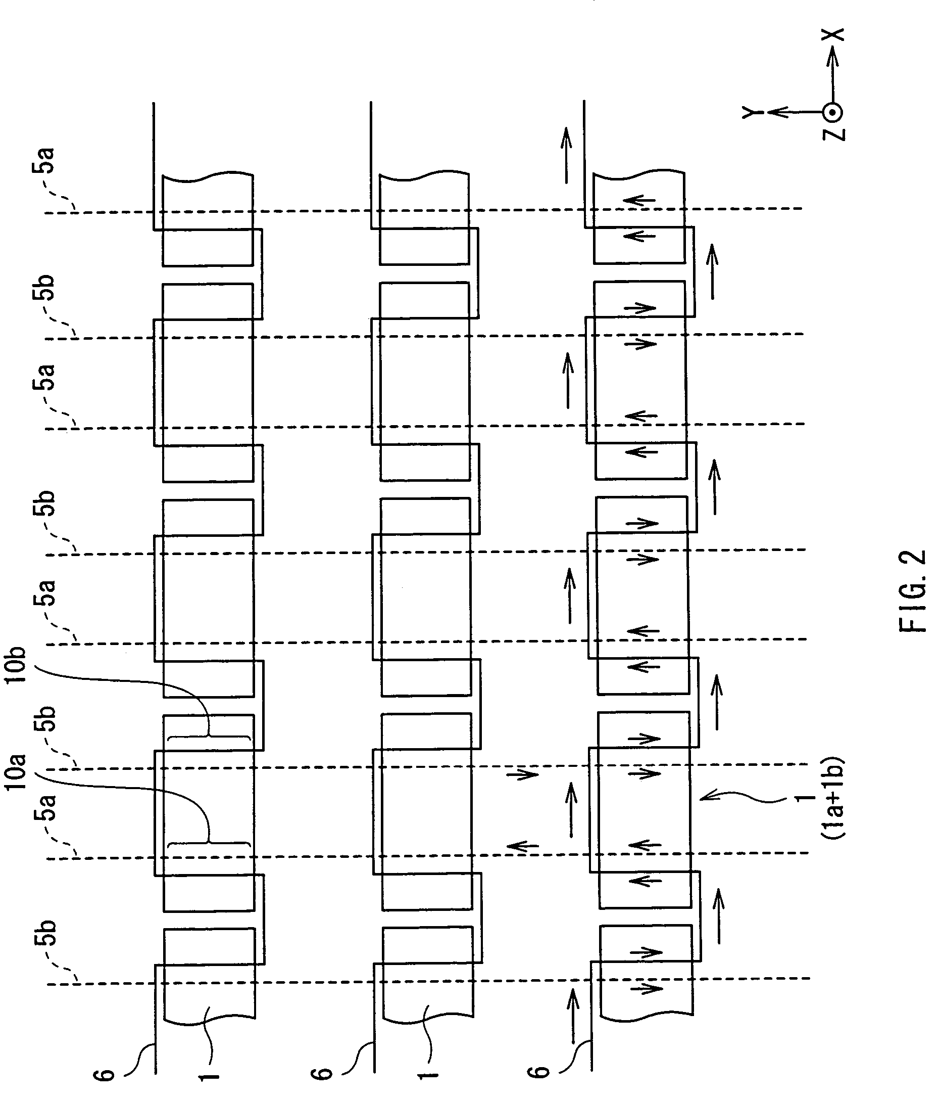
[0053]The memory cell group 54 has a matrix structure in which a number of memory cells 1 each having a pair of tunneling magneto-resistive elements (hereinbelow, called TMR elements) are arranged in a word line direction (X-direction) and a bit line direction (Y-direction) which are orthogonal to each other. The memory cell 1 is the minimum uni...


PUM


Abstract

The present invention provides a magnetic memory device capable of stably writing information by efficiently using a magnetic field generated by current flowing in a conductor, which can be manufactured more easily, and a method of manufacturing the magnetic memory device. The method includes: a stacked body forming step of forming a pair of stacked bodies S20a and S20b on a substrate 31; a lower yoke forming step of forming a lower yoke 4B so as to cover at least the pair of stacked bodies S20a and S20b; and a write line forming step of simultaneously forming a pair of first parts 6F and write bit lines 5a and 5b so as to be disposed adjacent to each other in a first level L1 via an insulating film 7A as a first insulating film on the lower yoke 4B. Thus, the manufacturing process can be more simplified.

Description

BACKGROUND OF THE INVENTION[0001]1. Field of the Invention[0002]The present invention relates to a magnetic memory device having a magnetoresistive element including a magneto-sensitive layer whose magnetization direction changes according to an external magnetic field and recording / reading information by using a change in the magnetization direction of the magneto-sensitive layer and to a method of manufacturing the same.[0003]2. Description of the Related Art[0004]Conventionally, as general memories used for an information processor such as a computer or a communication device, volatile memories such as a DRAM (Dynamic Random Access Memory) and an SRAM (Static RAM) are used. The volatile memories have to be refreshed by always supplying current to hold stored information. When the power source is turned off, all of information is lost, so that a nonvolatile memory as means for recording information has to be provided in addition to the volatile memory. For example, a flash EEPROM,...

Claims


Application Information

Patent Timeline
Patent Type & Authority Patents(United States)
IPC IPC(8): H01L29/76H01L29/94H01L31/113H01L31/119G11C11/15G11C11/16H01L21/8246H01L27/105H01L27/22H01L43/08
CPCH01L27/224G11C11/16H10B61/10
Inventor KAMIJIMA, AKIFUMI
Owner TDK CORPARATION
Why Eureka
Try Eureka