
Novel magnetic tunnel junction device and magnetic random access memory

a magnetic tunnel junction and random access memory technology, applied in semiconductor devices, digital storage, instruments, etc., can solve the problems of difficult switching of the ferromagnetic layer under an applied current, achieve enhanced antiferromagnetic coupling strength of the pinned layer based on the synthetic antiferromagnetic, and reduce the thickness of the ferromagnetic layer of the pinned layer

Inactive Publication Date: 2019-01-17
XI AN JIAOTONG UNIV
View PDF4 Cites 4 Cited by
  • Summary
  • Abstract
  • Description
  • Claims
  • Application Information

AI Technical Summary

Benefits of technology

This patent is about a device called a synthetic antiferromagnetic device that is used in a magnetic tunnel junction to improve data stability and reduce power consumption in a memory device. The device uses an electric field to enhance the coupling between two magnetic layers, ensuring that the data is written stably without being falsified. By reducing the thickness of the layer and increasing the arrangement density of the memory cells, the device can achieve higher data storage capacity and stability with lower power consumption. Overall, this invention improves the performance of magnetic memory devices and expands their applications.

Problems solved by technology

wherein the synthetic antiferromagnetic device is under an antiferromagnetic state; when the synthetic antiferromagnetic device adopts a material of a different type, a different thickness or a different interface disorder, an antiferromagnetic coupling strength is enhanced as an applied electric field strength increases; meanwhile, the ferromagnetic layer is difficult to be switched under an applied current.

Method used


Image

  • Novel magnetic tunnel junction device and magnetic random access memory
  • Novel magnetic tunnel junction device and magnetic random access memory
  • Novel magnetic tunnel junction device and magnetic random access memory

Examples


Embodiment Construction

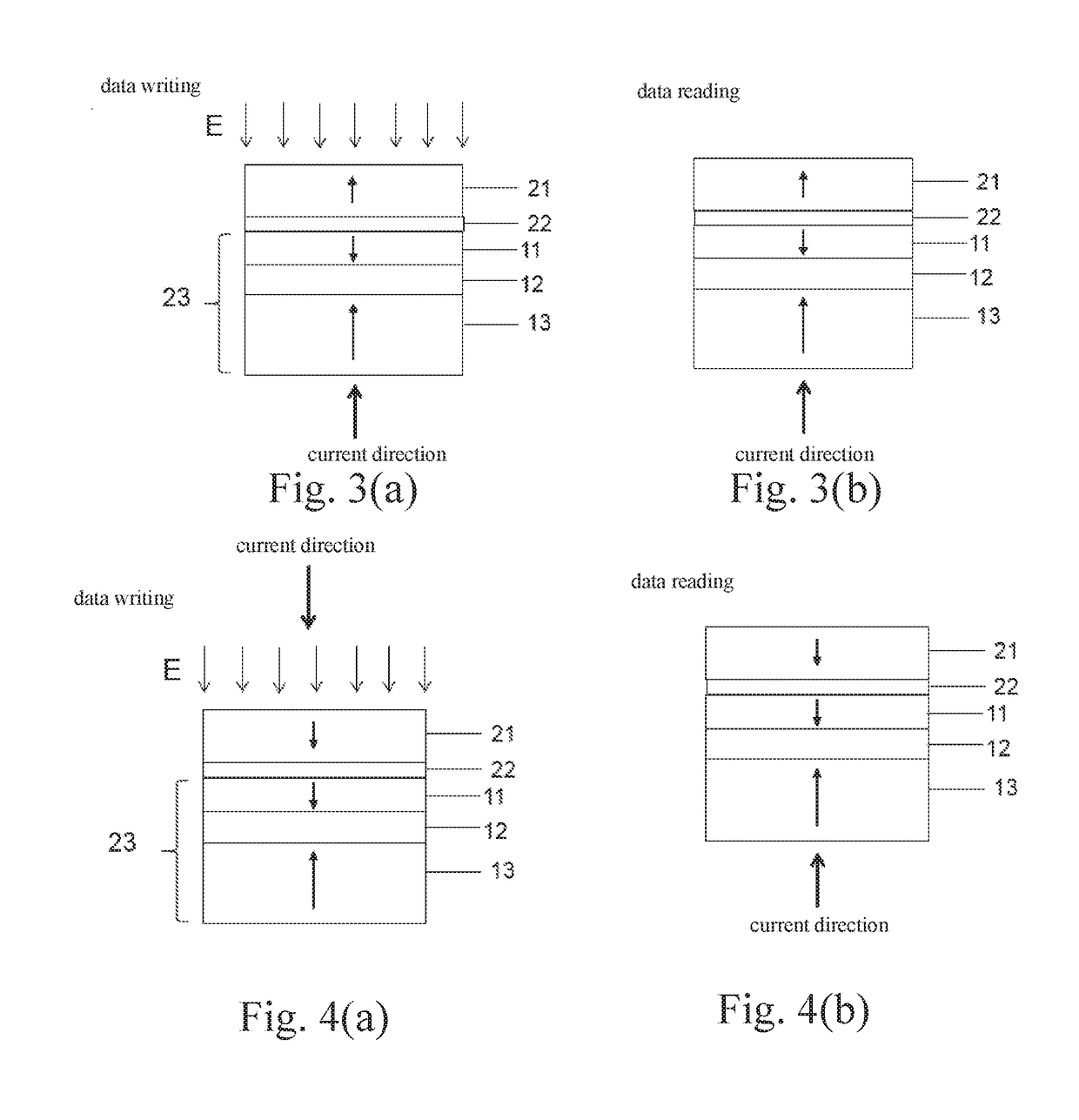
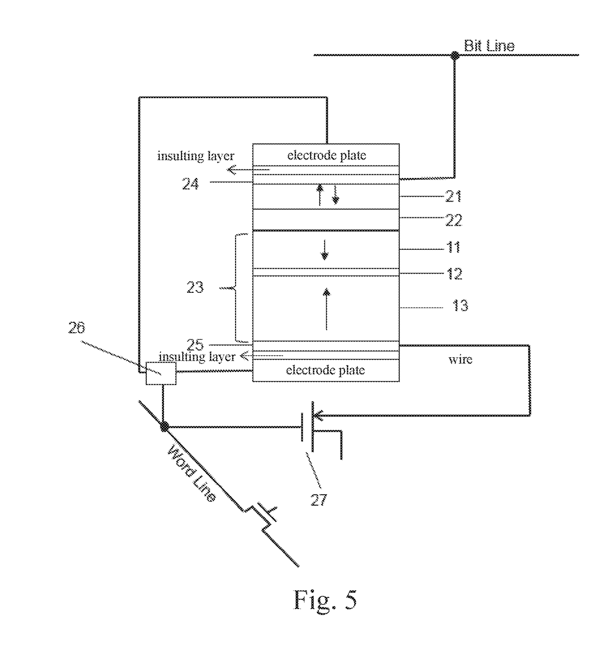
[0043]Referring to the accompanying drawings and embodiments, technical solution of the present invention will be described in detail below. The following embodiments relate to a magnetic random access memory for enhancing antiferromagnetic coupling of a synthetic antiferromagnetic pinned layer by electric field control, which are exemplary only and not intended to be limiting.

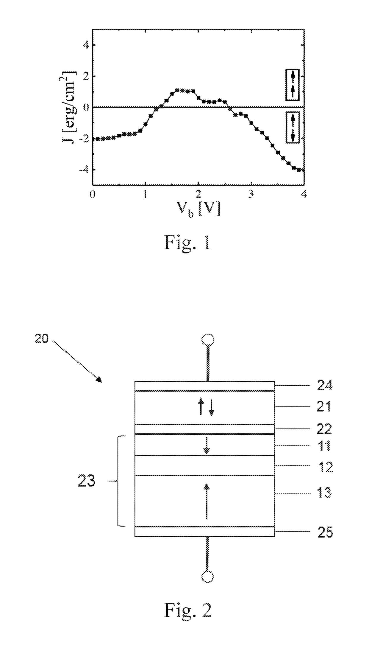
[0044]FIG. 1 illustrates variation of an antiferromagnetic coupling strength J of a synthetic antiferromagnetic device under voltage control, which is described in paper “Low voltage switching of magnetism through ionic liquid gating control of RKKY interaction in FeCoB / Ru / FeCoB and (Pt / Co)2 / Ru / (Co / Pt)2 multilayers”. When a ferromagnetic layer is [Pt (0.88 nm)|(Co(0.70 nm)]2, an interface disorder is 0.5, and a thickness of Ru is 0.66 nm, the synthetic antiferromagnetic device has relatively weak antiferromagnetic coupling in an initial state, and the antiferromagnetic coupling can be enhanced when an applied ...


PUM


Abstract

A magnetic tunnel junction device and a magnetic random access memory based on a synthetic antiferromagnetic pinned layer are disclosed, relating to a multilayer structure which is suitable for a pinned layer, namely a synthetic antiferromagnetic device. Antiferromagnetic coupling of the synthetic antiferromagnetic device can be enhanced by electric field. The synthetic antiferromagnetic device can be used as a pinned layer of the magnetic tunnel junction, and the antiferromagnetic coupling is enhanced under the electric field to ensure that a ferromagnetic layer, which is close to a barrier layer, of the pinned layer will not be switched, thereby achieving stable data writing. The magnetic random access memory is formed by the magnetic tunnel junction based on the synthetic antiferromagnetic pinned layer, has advantages such as, high density, low power consumption, high speed, radiation resistance and non-volatility.

Description

CROSS REFERENCE OF RELATED APPLICATION[0001]The present invention claims priority under 35 U.S.C. 119(a-d) to CN 201810837874.0, filed Jul. 26, 2018.BACKGROUND OF THE PRESENT INVENTIONField of invention[0002]The present invention relates to circuits and devices having magnetic / ferromagnetic materials or structures and applications thereof, and more particularly to an electrical-assist-controlled magnetic random access memory based on a synthetic antiferromagnetic pinned layer and using an electric field for auxiliary erasing.Description of Related Arts[0003]A magnetic tunnel junction (MTJ) consists of two magnetic metal layers (such as iron, cobalt, nickel) and an ultra-thin insulating layer (such as alumina or magnesia) sandwiched between two magnetic metal layers. If a bias voltage is applied between the two magnetic metal layers, since the insulating layer is thin, electrons can pass through the barrier through the tunneling effect. With a given bias voltage, the magnitude of the...

Claims


Application Information

Patent Timeline
Patent Type & Authority Applications(United States)
IPC IPC(8): H01L43/02H01L27/22H01L43/10H10N50/10H10N50/80
CPCH01L43/02H01L43/10H01L27/228G11C11/161H10N50/10H10B61/22H10N50/85H10N50/80
Inventor MIN, TAIZHOU, XUEWANG, LEI
Owner XI AN JIAOTONG UNIV
Learn More