Interferometric measuring device and projection exposure installation comprising such measuring device

a technology of interferometry and measuring devices, which is applied in the direction of photomechanical equipment, instruments, originals for photomechanical treatment, etc., can solve problems such as the optical properties of the device, and achieve the effect of simple structure, rapid and fault-free measuremen

Inactive Publication Date: 2007-01-02
CARL ZEISS SMT GMBH
View PDF38 Cites 19 Cited by
  • Summary
  • Abstract
  • Description
  • Claims
  • Application Information

AI Technical Summary

Benefits of technology

[0008]It is an object of the invention to provide an interferometric measuring device of the type mentioned at the beginning which is distinguished by a simple structure in the region of the wavefront source. It is another object to provide a measuring device which is capable of being integrated into a microlithographic projection exposure installation in a simple manner and which permits rapid and fault-free measurements on projection objectives in their operating state.
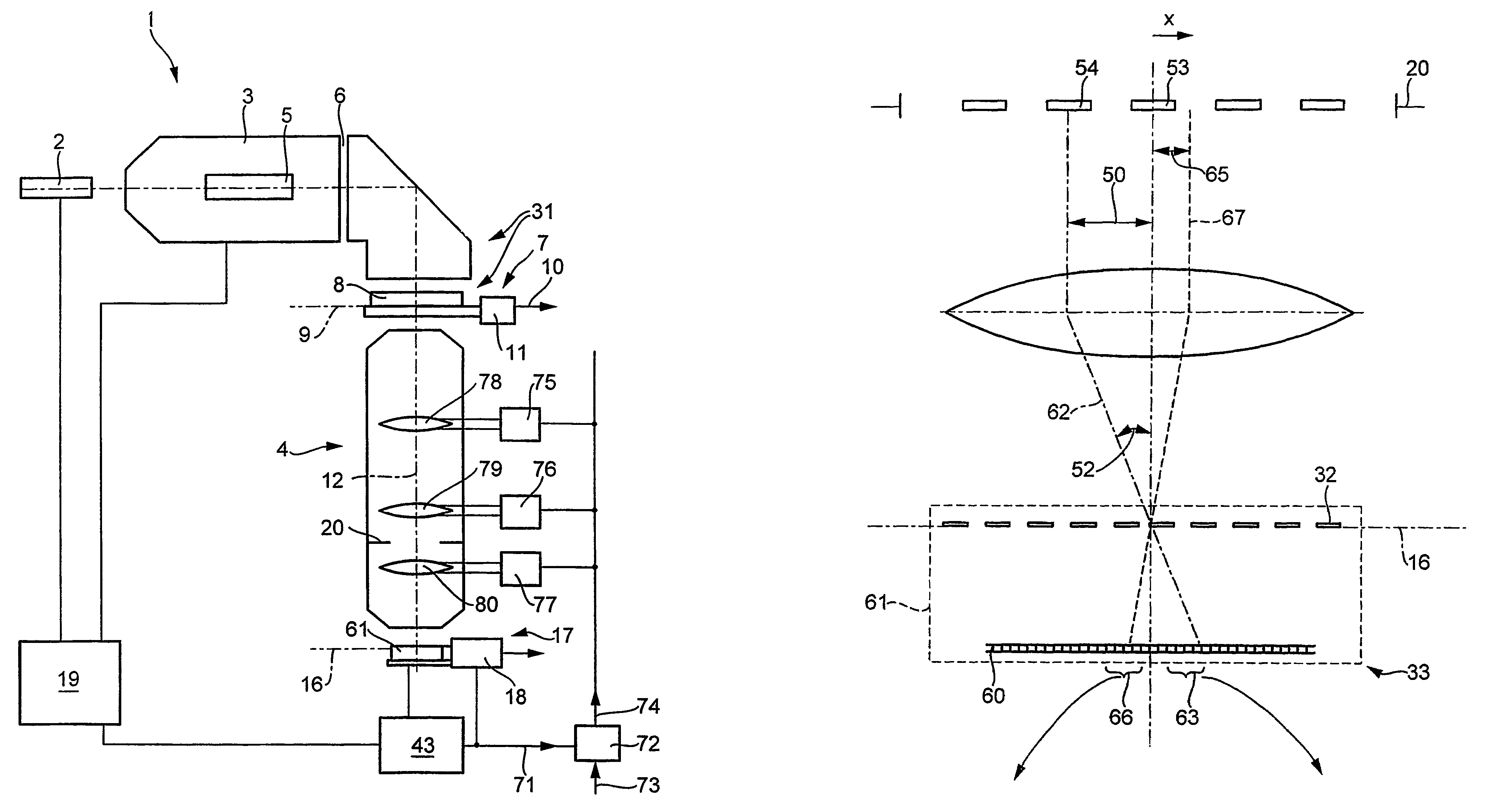
[0014]It is thus possible to integrate the measuring structures for the interferometer, which were conventionally present in a separate measuring reticle, in the usual reticles for the chip structures. This therefore dispenses with the need, before an interferometric measurement of a projection objective, to replace the chip production reticle used during the chip production by a separate measuring reticle (for example a wavefront module). Instead, the measuring pattern which, because of its coherence-shaping properties, can also be designated a “coherence pattern”, is provided as part of the reticle used for the production of structured components, on this reticle. As a result, the costs for the provision of an interferometric measuring device can be reduced considerably. In addition, interferometric measurements on incorporated objectives are faster than was previously possible, which reduces the machine downtimes and as a result increases the productivity of the projection exposure installation. Moreover, it is possible in a particularly simple manner to obtain measuring data relating to projection objectives in good time in relation to the production process, in order for example to be able to counteract worsening of the imaging quality in good time by means of suitable manipulations of the projection objective. Using measuring devices according to the invention, it is merely necessary, for the measurement, to replace the component arranged in the region of the image plane of the projection objective and to be exposed, for example a semiconductor wafer, for a short time by a diffraction grating matched to the measuring structure. The spatially resolving detector can be integrated permanently in the projection exposure installation or be capable of being replaced or interchanged together with the diffraction grating.
[0018]The diffraction grating, which can likewise be one-dimensionally or two-dimensionally periodic, is preferably formed as a function of the structure of the measuring pattern in such a way that only specific diffraction orders contribute to the interference at the diffraction grating, for example only the zeroth and first diffraction orders. All of the diffraction grating types mentioned in DE 101 09 929, such as phase gratings, amplitude gratings or reflective gratings, are possible. Diffraction gratings which in each case have a diffractive, periodic structure for different directions are preferred, which makes it possible to determine phase gradients in more than one direction from individual interferograms. Diffraction gratings with periodicity directions running orthogonally to one another, for example chessboard gratings or crossed gratings, are favourable, but also possible are gratings with other symmetries, for example with angles of 45°, 60° or 120° between periodicity directions.
[0021]According to a development, provision is made for the mask, in at least one region, to have a scattering structure for homogenizing the intensity distribution in the light path of the scattering structure and, if appropriate, for reducing the spatial coherence of the illuminating light. The scattering structure can bring about a change in the etendue of the radiation, in that angles of light rays which were previously not present are added and / or the existing angular distribution is modified. The scattering structure can have a statistical distribution of scattering centers, such as in the case of a matt disk. It is also possible for there to be regularly distributed scattering centers, for example in the form of crossed cylindrical lenses. These can be irregular or regular structures which, for example, are produced by etching or another surface-roughening treatment. In addition, computer-generated holograms (CGH) are also possible as scattering structures. Scattering structures on the reticle can make it possible, for example, to measure an imaging system at its full numerical aperture, even if the illumination system connected upstream has a smaller numerical aperture. With the aid of the scattering, in this case otherwise unexposed regions of the pupil can also be illuminated. In this way, scattering structures between illumination system and system to be measured can have an enabling effect as a result of introducing further angles.
[0027]Given adequate lateral extent of the parcels or of the regions of high intensity in the pupil plane of the imaging system, it can also be beneficial to set a shearing distance which is small as compared with the extent of the parcels. As a result, two or more points within an intensity maximum of the illumination intensity can be compared largely free of intensity and modulation fluctuations.

Problems solved by technology

Since, on account of the complicated optical structure, it is as a rule impossible to derive the optical properties of the objectives from theoretical calculations, the optical properties have to be measured reliably, at least during the assembly and the adjustment of the optical imaging systems.

Method used


Image

  • Interferometric measuring device and projection exposure installation comprising such measuring device
  • Interferometric measuring device and projection exposure installation comprising such measuring device
  • Interferometric measuring device and projection exposure installation comprising such measuring device

Examples


Embodiment Construction

[0038]FIG. 1 shows in schematic form a microlithography projection exposure installation in the form of a wafer stepper 1, which is provided for the production of highly integrated semiconductor components. The projection exposure installation comprises an excimer laser 2 as the light source, which emits light with an operating wavelength of 248 nm, it being possible for the operating wavelength in other embodiments also to lie below this, for example at 193 nm or 157 nm, or above this. There are also systems which operate with shorter wavelengths from the EUV range and corresponding light sources. An illumination system 3 connected downstream generates a large, sharply delimited and homogeneously illuminated image field, which is adapted to the telecentric requirements of the projection objective 4 connected downstream. The projection objective 4 is a preferred embodiment of an optical imaging system to be measured. The illumination system has devices for selecting the illuminating...


PUM

PropertyMeasurementUnit
wavelengthsaaaaaaaaaa
operating wavelengthaaaaaaaaaa

Abstract

A measuring device for interferometric measurement of an optical imaging system that is provided for projecting a useful pattern, provided on a mask, into the image plane of the imaging system, includes a wavefront source for generating at least one wavefront traversing the imaging system; a diffraction grating, arrangeable downstream of the imaging system, for interacting with the wavefront reshaped by the imaging system; and a spatially resolving detector, assigned to the diffraction grating, for acquiring interferometric information. The wavefront source has at least one measuring pattern that is formed on the mask in addition to the useful pattern. The useful pattern may represent the structure of a layer of a semiconductor component in a specific fabrication step. The measuring pattern may be formed as a coherence-forming structure periodic in one or two dimensions.

Description

[0001]This application is a Continuation of International Application PCT / EP03 / 03566 filed Apr. 5, 2003, and claiming priority of German Patent Application 102 17 242.0 filed Apr. 15, 2002. The disclosure of International Application PCT / EP03 / 03566 is incorporated herein by reference.BACKGROUND OF THE INVENTION[0002]1. Field of the Invention[0003]The invention relates to a measuring device for interferometric measurement of an optical imaging system and to a microlithographic projection exposure installation in which such a measuring device is integrated.[0004]2. Discussion of the Related Art[0005]Higher and higher requirements are being placed on the imaging quality of optical imaging systems. One example of this is projection objectives for microlithographic production of semiconductor components and other finely structured components which are intended to produce structures in the sub-micrometer range largely free of imaging errors. Since, on account of the complicated optical st...

Claims


Application Information

Patent Timeline
Patent Type & Authority Patents(United States)
IPC IPC(8): G01B9/02G02B5/02G03F1/08G03F7/20H01L21/027
CPCG02B5/0221G03F7/706G03F7/70075G02B5/0252
Inventor SCHRIEVER, MARTINWEGMANN, ULRICHHAIDNER, HELMUT
Owner CARL ZEISS SMT GMBH
Why Eureka
Try Eureka