
Module component

Active Publication Date: 2007-01-09
SAMSUNG ELECTRONICS CO LTD
View PDF18 Cites 59 Cited by
  • Summary
  • Abstract
  • Description
  • Claims
  • Application Information

AI Technical Summary

Benefits of technology

[0004]A module includes a component, a circuit board having the component mounted thereon, a first grounding pattern formed on an outermost periphery of a surface portion of the circuit board; a first sealer provided on the circuit board and having a dimension projected on the circuit board, an

Problems solved by technology

Metal case 22 may contact component 23 mounted on circuit board 21, thus causing short-circuiting, or may apply an external stress to the board, thus causing malfunction of a circuit.
This structure prevents the module from being thin and from manufactured easily, and prevents the case from providing a sufficient shielding effect.

Method used


Image

  • Module component
  • Module component
  • Module component

Examples


exemplary embodiment 1

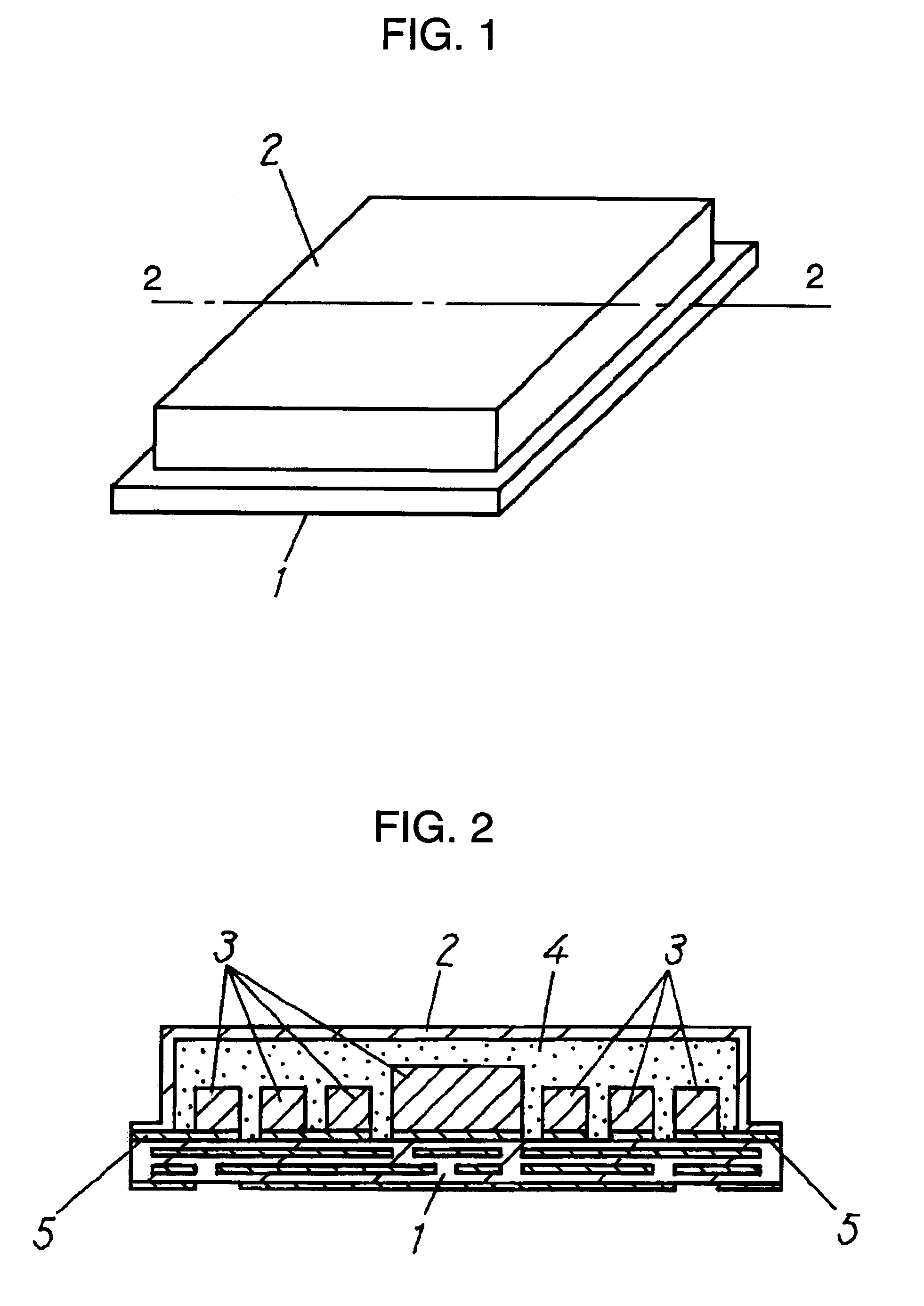
[0015]FIG. 1 is a perspective view of a component module in accordance with Exemplary Embodiment 1 of the present invention. FIG. 2 is a cross-sectional view of the module at line 2—2 shown in FIG. 1. Circuit board 1 is made of a multi-layer printed circuit board including at least two wiring layers having a power supply circuit, a grounding pattern, and a high-frequency circuit formed on the layers. Components 3, such as a resistor, a capacitor, a coil, a semiconductor, and a crystal connected to the board with lead-free solder are mounted on circuit board 1. Sealer 4 made of epoxy resin has a dimension projected on board 1 smaller than an outer dimension of circuit board 1 and is formed on circuit board 1 and covers components 3. Metal film 2 is provided on sealer 4. Metal film 2 is connected to first grounding pattern 5 formed on four sides of an outermost periphery of a surface portion 1A of circuit board 1.

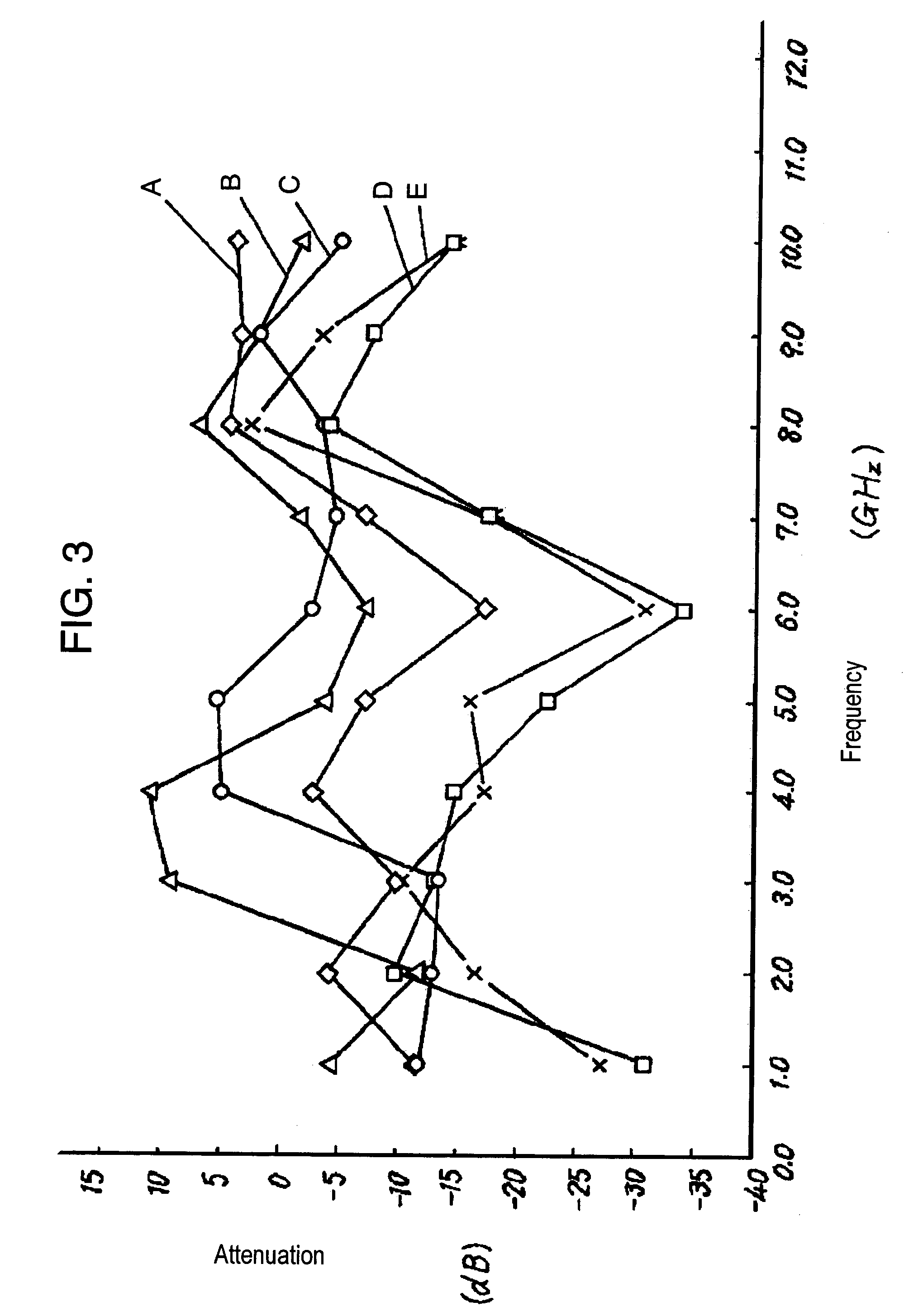
[0016]FIG. 3 is a chart for comparing shielding effects of various compo...

exemplary embodiment 2

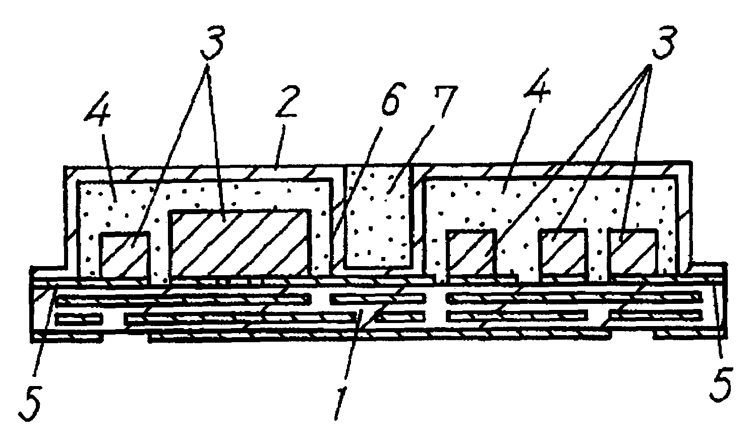
[0024]FIG. 5 is a perspective view of a component module in accordance with Exemplary Embodiment 2 of the present invention. FIG. 6 is a cross-sectional view of the module at line 6—6 shown in FIG. 5. As illustrated in FIG. 5, in the module in accordance with Embodiment 2, sealer 4 covered with metal film 2 is divided into three blocks by sealer 7 made of second resin.

[0025]As shown in FIG. 6, a power supply circuit, a ground pattern and a high-frequency circuit described in Embodiment 1 are formed on at least two wiring layers of circuit board 1. First grounding pattern 5 is formed on an outer periphery of the circuit board.

[0026]Components 3, such as a resistor, a capacitor, a transistor, and a crystal are mounted on circuit board 1. Sealer 4 covering components 3 has a dimension projected on circuit board 1 which is smaller than an outer dimension of circuit board 1 and is formed on circuit board 1. Sealer 4 has dividing ditch 6 provided therein for separating the circuit board i...


PUM


Abstract

A module includes a component, a circuit board having the component mounted thereon, a first grounding pattern formed on an outermost periphery of a surface portion of the circuit board; a first sealer provided on the circuit board and having a dimension projected on the circuit board, and a metal film covering the sealer and connected to the grounding pattern. The dimension of the first dealer is smaller than an outside dimension of the circuit board. The first sealer is made of first resin and sealing the component. The module has a low profile and is adequately shielded.

Description

TECHNICAL FIELD[0001]The invention relates to a component module used for various electronic equipment and communications equipment.BACKGROUND ART[0002]A conventional component module illustrated in FIG. 9 includes circuit board 21 mounting component 23 at least on a side of the board, grounding electrode 24 having a recess shape formed on a side of circuit board 21, and metal case 22 covering mounted component 23. Metal case 22 has a terminal inserted and connected to grounding electrode 24 with a solder to electrically shield the module.[0003]Since metal case 22 is soldered to the side of circuit board 21 of the conventional component module, circuit board 21 needs to have a thickness to support metal case 22. Metal case 22 may contact component 23 mounted on circuit board 21, thus causing short-circuiting, or may apply an external stress to the board, thus causing malfunction of a circuit. Therefore, metal case 22 is taller than component 23 for avoiding such incidents. Additiona...

Claims


Application Information

Patent Timeline
IPC IPC(8): H01L23/28H01L21/60H01L23/31H01L23/552H01L23/60H05K1/02H05K3/28
CPCH01L23/3121H01L23/552H05K3/284H01L23/60H01L2924/00011H01L2224/293H01L2224/2929H05K1/0218H01L2924/3025H01L2924/19105H01L24/83H01L2224/83851H01L2924/19041H01L2224/29075H01L2924/00014
Inventor TSUNEOKA, MICHIAKIHASHIMOTO, KOJIHAYAMA, MASAAKIYASUHO, TAKEO
Owner SAMSUNG ELECTRONICS CO LTD
Learn More