
Programmable logic device

a logic device and programmable logic technology, applied in the field of programmable logic devices, can solve the problems of high price, high price of programmability in the form of a memory with conversion into switched data paths, and high cost of programmability in the form of a memory with conversion into switched data paths, and achieve the effect of high functional density and high speed of the pld

Inactive Publication Date: 2007-01-09
SIEMENS AG
View PDF8 Cites 10 Cited by
  • Summary
  • Abstract
  • Description
  • Claims
  • Application Information

AI Technical Summary

Benefits of technology

[0013]It is, therefore, the object of the present invention to design the programmable logic device having the features initially mentioned in such a manner that, with a high functional density, a high speed of the PLD can be achieved by simple means.
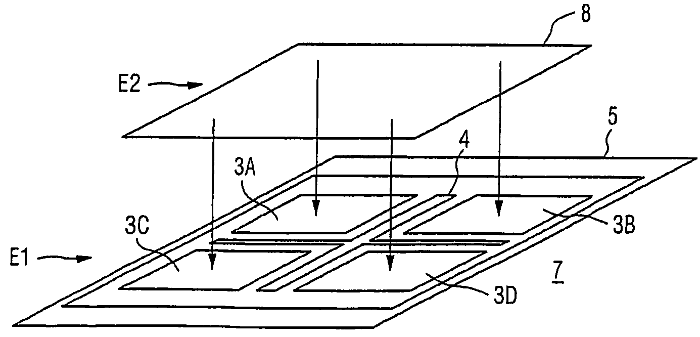
[0016]In this arrangement, the configuring can be performed at any time, i.e. during the entire uninterrupted period of operation—that is to say not only during a start-up or boot phase. The measures according to the invention thus mean a connection from the changeover logic block to linking areas and thus to a corresponding configuration of these. This makes it possible for different functions to be executed at different times by individual blocks; i.e. their utilization is correspondingly increased. This is associated with a corresponding improvement in performance of the entire logic device compared with a microprocessor or, respectively, no loss of performance in comparison with conventional PLDs.
[0022]It is also of advantage if at least some of the reconfigurable logic blocks are configured in accordance with a predetermined context.

Problems solved by technology

This type of storage is complex because a quantity of additional transistors must be added around the memory itself for the purpose of quick conversion into switched data paths.
Since the programmability in the form of a memory with conversion into switched data paths is quite expensive as in the case of the computer, but the complete program has hitherto been stored in a chip, the PLDs, in spite of a potential for high functional density, “only” achieve a factor of 10 more than processors.
This means that the gain in speed in PLDs compared with processor solutions comes at a high price.

Method used


Image

  • Programmable logic device
  • Programmable logic device
  • Programmable logic device

Examples


example

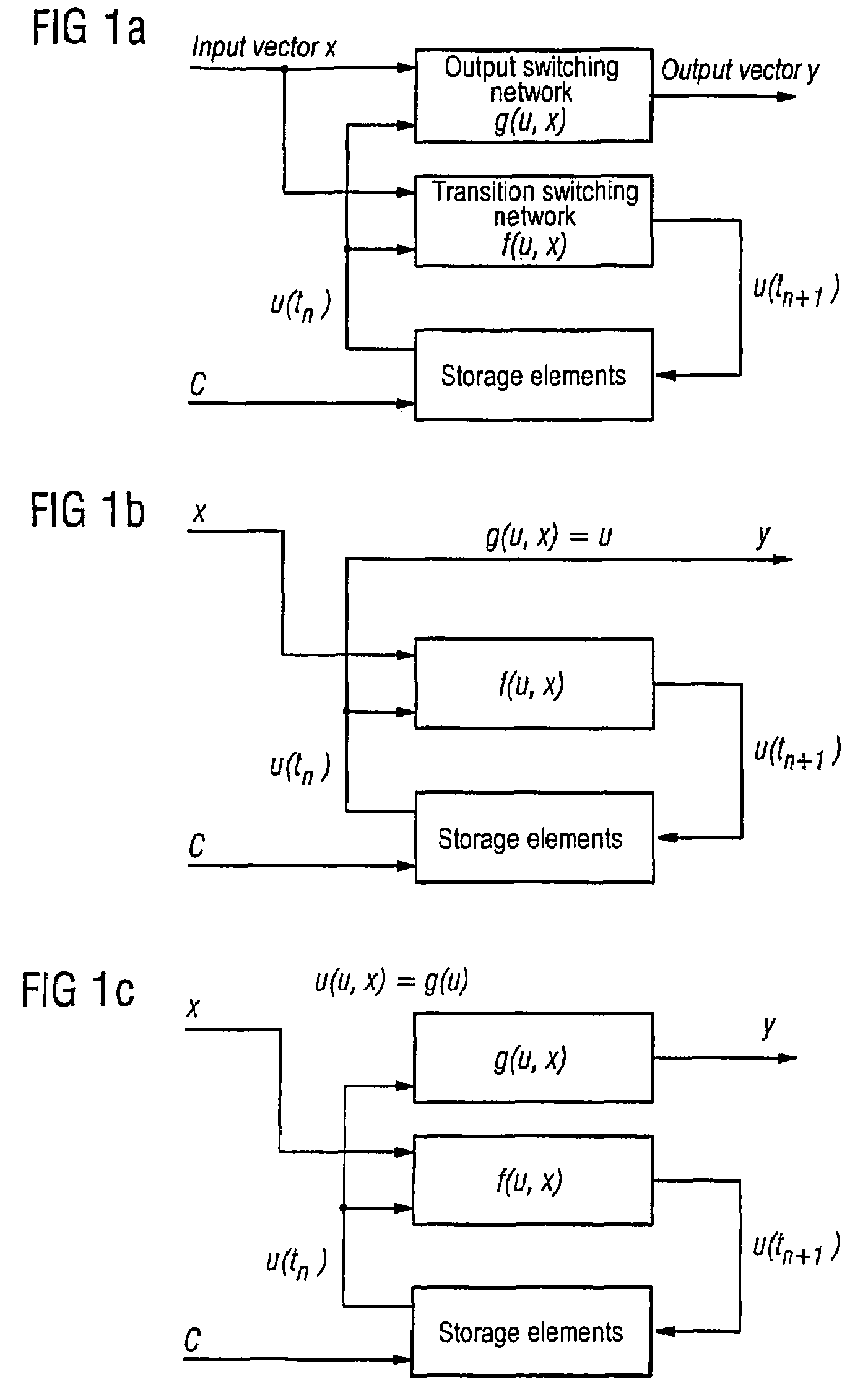
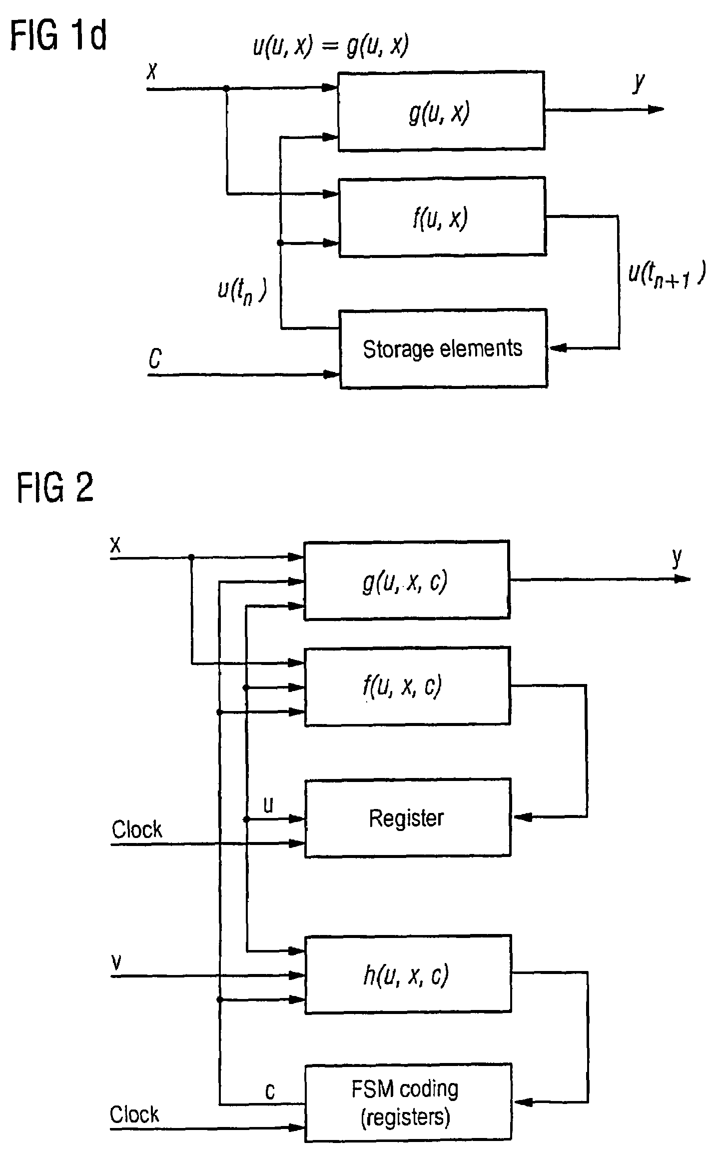
[0055]The road traffic light, which is a favorite example of a Finite State Machine, can also provide a very good example of a sequential FSM if a night mode is considered. The word mode indicates the approach: the switching between individual FSMs should include something like a mode change, and day and night mode are mutually exclusive.[0056]FSM1 then integrates the day light, FSM2 integrates the night light (e.g. amber flashing for the side roads) and in the higher-level sequencer a timing signal is used for deciding which FSM will be executed and which is idle. The sequencer is implemented as FSM0.[0057]The three FSMs (0 . . . 2) required for this are described separately but then integrated on one PLD so that FMS0 would be in area 0, FSM1 in 1 and FSM2 in 2. This would not result in a gain in area.[0058]In the reloadable case, FSM0 would have to be available permanently, and also an area which could accommodate the maximum of {FSM1, FSM2}. In this area, one of two would then be...


PUM


Abstract

The invention relates to a programmable logic device (7) comprising several logic blocks (3A to 3D) with configurable characteristics, elements for linking the logic blocks to one another and a processing unit (4) and an input / output unit (5). In addition, the linking elements have at least one configurable changeover logic block, enabling the logic blocks (3A to 3D) to be re-configured during the operation of the logic device (7). Said changeover logic block is used for the configuration of at least one of the re-configurable logic blocks (3A to 3D) and its connection to other blocks and / or its connection to the processing unit (4) and / or to the input / output unit (5).

Description

CONTINUATION DATA[0001]This application is a 371 of PCT / IDE03 / 03524 filed on Oct. 23, 2003.CROSS REFERENCE TO RELATED APPLICATIONS[0002]This is the 35 USC 371 national stage of international application PCT / DE2003 / 003524, filed on 23 Oct. 2003, which designated the United States of America.FIELD OF THE INVENTION[0003]The invention relates to a programmable logic device having a number of logic blocks with configurable characteristics which in each case comprise at least one logic processing unit with function programs and interfaces to the other logic blocks in each case, comprising at least one input and output unit allocated to the logic blocks and having means for linking the logic blocks to one another, to the at least one processing unit of another logic block and to the at least one input / output unit. Such a logic device can be found in U.S. Pat. No. 4,870,302 A.BACKGROUND OF THE INVENTION[0004]Programmable logic chips of conventional logic devices such as, in particular, proc...

Claims


Application Information

Patent Timeline
Patent Type & Authority Patents(United States)
IPC IPC(8): H03K19/177
CPCH03K19/17736H03K19/17796H03K19/17756H03K19/17752
Inventor SIEMERS, CHRISTIAN
Owner SIEMENS AG
Learn More