Eureka AIR delivers breakthrough ideas for toughest innovation challenges, trusted by R&D personnel around the world.

Three-dimensional capacitor inductor based on high-functional-density silicon through hole structure and preparation method

A technology of three-dimensional capacitors and through-silicon vias, which is applied to circuits, electrical components, and electrical solid-state devices, can solve problems such as single function, low utilization rate, and large area, so as to improve functional density, utilization rate, and integration. Effect

Active Publication Date: 2020-10-13
FUDAN UNIV +1
View PDF2 Cites 1 Cited by
  • Summary
  • Abstract
  • Description
  • Claims
  • Application Information

AI Technical Summary

Problems solved by technology

These structural TSVs occupy a large area of ​​silicon and have a single function
Therefore, the functional density of TSV is very low and the utilization of silicon is very low

Method used


Image

  • Three-dimensional capacitor inductor based on high-functional-density silicon through hole structure and preparation method
  • Three-dimensional capacitor inductor based on high-functional-density silicon through hole structure and preparation method
  • Three-dimensional capacitor inductor based on high-functional-density silicon through hole structure and preparation method

Examples


Embodiment Construction

[0031] In order to make the purpose, technical solutions and advantages of the present invention clearer, the technical solutions in the embodiments of the present invention will be clearly and completely described below in conjunction with the accompanying drawings in the embodiments of the present invention. It should be understood that the specific The examples are only used to explain the present invention, not to limit the present invention. The described embodiments are only some, not all, embodiments of the present invention. Based on the embodiments of the present invention, all other embodiments obtained by persons of ordinary skill in the art without making creative efforts belong to the protection scope of the present invention.

[0032] In the description of the present invention, it should be noted that the orientation or positional relationship indicated by the terms "upper", "lower", "vertical" and "horizontal" are based on the orientation or positional relation...


PUM


Abstract

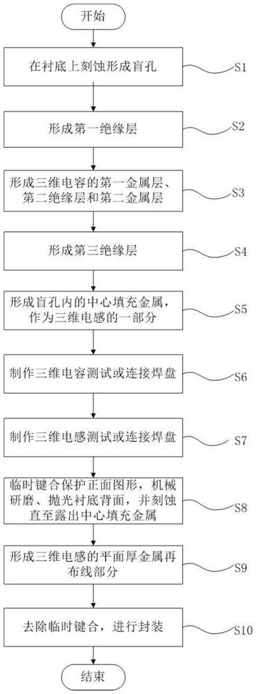
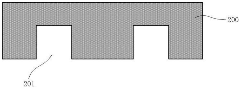
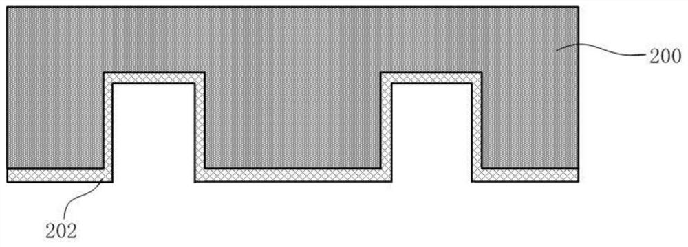
The invention belongs to the technical field of semiconductor devices, and particularly relates to a three-dimensional capacitor inductor based on a high-functional-density silicon through hole structure and a preparation method. The three-dimensional capacitor inductor comprises a substrate, provided with a silicon through hole; a three-dimensional capacitor, formed on the side wall of the silicon through hole and sequentially comprising a first metal layer, a second insulating layer and a second metal layer; a three-dimensional inductor, formed by rewiring central filling metal and planar thick metal of the silicon through hole. A first insulating layer is arranged between the side wall of the silicon through hole and the three-dimensional capacitor, and a third insulating layer is arranged between the three-dimensional capacitor and the three-dimensional inductor. Values of capacitance and inductance in an integrated system can be effectively increased, capacitance and inductance can be integrated near a chip in three-dimensional integration, the functional density of through silicon vias in three-dimensional integration can be improved, and the utilization rate of silicon in system integration is increased. Compared with discrete capacitors and inductors on other organic substrates, the integration level is greatly improved.

Description

technical field [0001] The invention belongs to the technical field of semiconductor devices, and in particular relates to a three-dimensional capacitive inductor based on a high functional density through-silicon hole structure and a preparation method thereof. Background technique [0002] With the increasing integration of integrated circuits, the feature size of devices has approached the physical limit. In order to further improve performance and integration, researchers began to continuously increase the utilization rate of silicon, that is, the functional density. Among them, the system integration of the chip in the three-dimensional direction can greatly improve the functional density of the chip, but as the chip density increases in the system integration, the signal coupling becomes extremely serious, and more and more decoupling capacitors and inductors are required. . Only relying on the capacitance and inductance on the PCB board cannot meet the requirements ...

Claims


Application Information

Patent Timeline
IPC IPC(8): H01L23/522H01L21/768
CPCH01L23/5227H01L23/5223H01L21/76898H01L21/76801H01L21/76838H01L21/76877H01L23/481H01L28/91H01L24/05H01L27/01H01L2224/05541H01L2224/05647H01L2224/05684
Inventor 张卫刘子玉陈琳孙清清
Owner FUDAN UNIV
Why Eureka
Eureka Blog
Learn More