Display panel and manufacturing method of display panel

a technology of display panel and manufacturing method, which is applied in the direction of identification means, instruments, individual semiconductor device testing, etc., can solve the problems of forming a deep hole in the panel, and affecting the appearance of the display panel. , to achieve the effect of preventing the intrusion of moistur

Active Publication Date: 2007-01-16
SANYO ELECTRIC CO LTD
View PDF2 Cites 6 Cited by
  • Summary
  • Abstract
  • Description
  • Claims
  • Application Information

AI Technical Summary

Benefits of technology

[0016]According to the present invention, before formation of a display element is completed, line disconnection is performed with regard to a defective pixel, and the defective pixel is darkened. Then, in the subsequent step of forming an insulating layer, a hole created by the line disconnection can be filled in. It is therefore possible to prevent the intrusion of moisture or the like in a completed display panel.
[0017]Further, according to the present invention, before formation of a display element is completed, a continuity test is performed, and line disconnection using laser, for example, is performed with regard to a defective pixel, and the defective pixel is darkened. Then, in the subsequent step of forming an insulating layer or the like, a hole created by the laser or the like can be repaired.

Problems solved by technology

In an organic EL panel as described above, the first TFT or the second TFT provided for each pixel may become defective.
When these first and second TFTs have a defect, there is a possibility that a pixel is displayed as a luminous dot (a pixel which never becomes dark) or a dark dot (a pixel which never becomes bright), or that the data line DL connected to these TFTs is affected by generation of a short circuit, thereby causing a defect in the line.
Although such a repair method results in a number of dark dots, this does not in itself significantly affect the usefulness of the organic EL panel as a product.
The repair treatment using YAG laser, however, results in formation of a deep hole in the panel.
While organic layers and a cathode are to be formed subsequently in the case of an organic EL panel, these layers are too thin to sufficiently cover the hole.
As a result, side surfaces of the organic layers of the organic EL element are also directly exposed to a space above the cathode, which may accelerate deterioration of the organic layers due to intrusion of moisture and may increase defective pixels.
As a result, side surfaces of each layer are exposed, often resulting in rapid deterioration and alignment disorders in a fine pixel device.

Method used


Image

  • Display panel and manufacturing method of display panel
  • Display panel and manufacturing method of display panel
  • Display panel and manufacturing method of display panel

Examples


Embodiment Construction

[0021]A preferred embodiment of the present invention will be described in further detail with reference to the accompanying drawings.

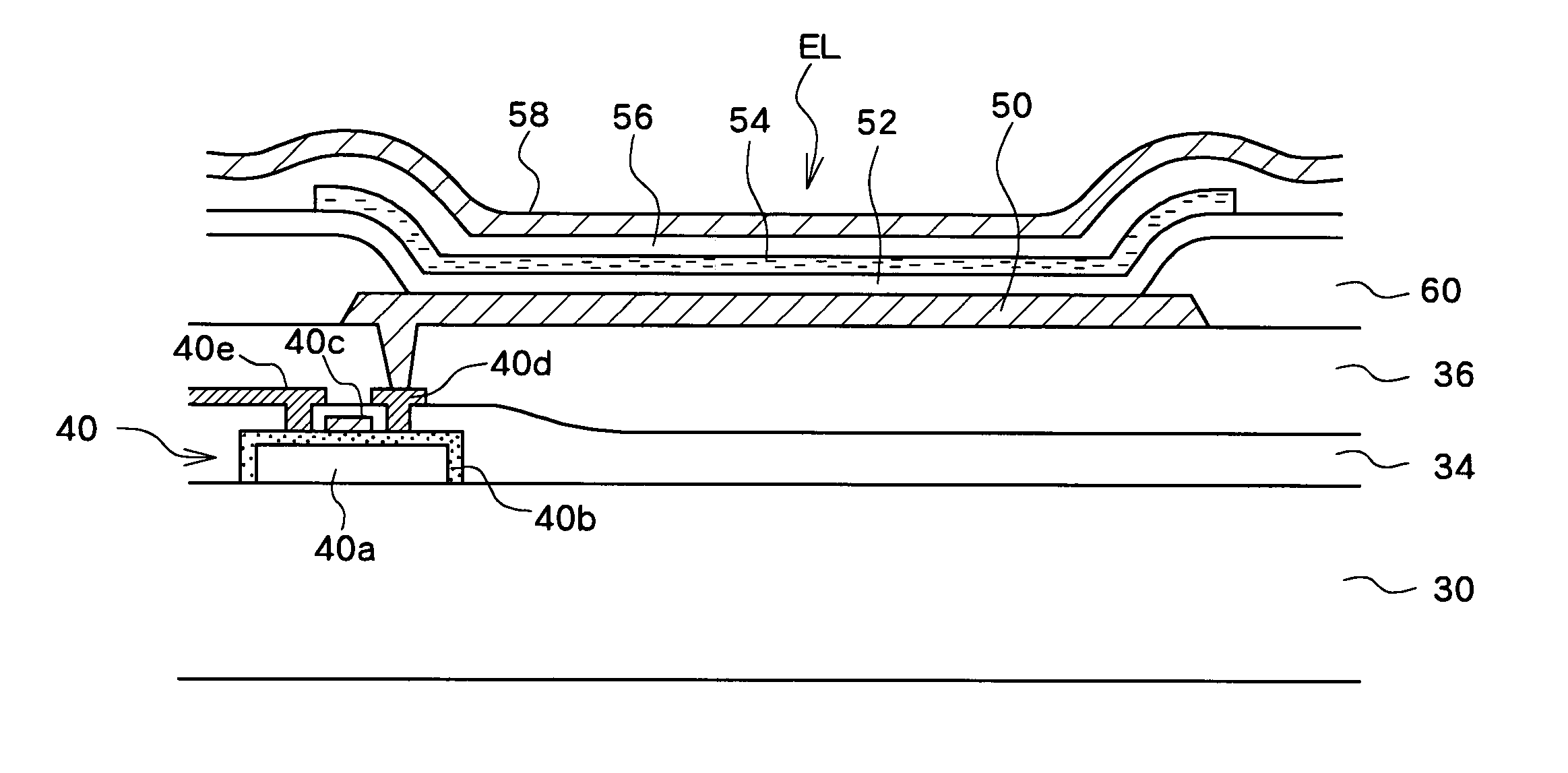
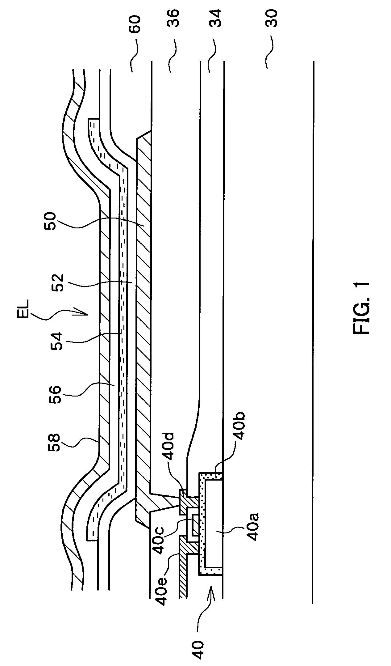
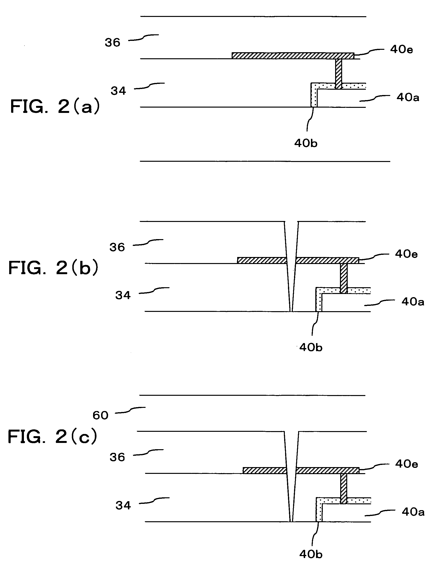
[0022]Referring to FIG. 1, manufacturing of a display apparatus in accordance with an embodiment of the present invention will be described. First, a TFT is formed on a glass substrate 30. More specifically, an active layer 40a made of low temperature polycrystalline silicon is formed, and a gate oxide film of silicon oxide is formed on the surface of the active layer to form a gate electrode 40c. Then, impurities are doped in the active region 40a using the gate electrode 40c as a mask, thereby forming source and drain regions. Further, after an interlayer insulating film 34 is formed to cover the TFT, contact holes are formed in the interlayer insulating film 34 for forming a source electrode 40d and a drain electrode 40e. Then, a planarization insulating film 36 is formed, and a contact hole communicating with the source electrode 40d is formed in ...


PUM

PropertyMeasurementUnit
wavelengthaaaaaaaaaa
thicknessaaaaaaaaaa

Abstract

An array test is performed during the process of panel formation, such as at a stage where a driving TFT which supplies a drive current for an organic EL element is completed and an anode of the organic EL element has been formed on the TFT. Then, with regard to a defective pixel, a line connecting the driving TFT and the anode is disconnected using a laser. After the line has been thus disconnected, a planarization insulating film is formed, and this film fills the holes caused by the laser irradiation. It is thus possible to suppress deterioration of pixels and also effectively darken a defective pixel using laser.

Description

BACKGROUND OF THE INVENTION[0001]1. Field of the Invention[0002]The present invention relates to manufacturing of an active matrix display panel including a display element and a thin film transistor (hereinafter referred to as TFT) which controls connection between the display element and a power source line, and more particularly to processing related to a defective pixel.[0003]2. Description of Related Art[0004]Organic electroluminescence (hereinafter referred to as “EL”) display panels have been conventionally known as one type of flat display panel. Unlike liquid crystal display panels (LCDs), organic EL display panels are self-emissive. This feature, as well as their brightness and clarity, has fueled expectations of their widespread use.[0005]Organic EL displays are composed of a great number of organic El elements, which function as pixels, arranged in a matrix. Further, of passive and active driving methods which can be used for organic EL elements as well as for LCDs, as i...

Claims


Application Information

Patent Timeline
Patent Type & Authority Patents(United States)
IPC IPC(8): H01L21/00G01R31/00G02F1/13G02F1/1333H05B33/10G02F1/1362G09F9/00G09F9/30H01L21/77H01L27/12H01L27/32H01L51/50H05B33/22
CPCH01L27/3244H01L27/1248H01L27/124G02F2001/136268H01L2251/568G02F1/136268H10K59/12H10K71/861H10K71/70H05B33/10
Inventor JINNO, YUSHI
Owner SANYO ELECTRIC CO LTD
Why Eureka
Try Eureka