Method and apparatus for observing a specimen

a specimen and method technology, applied in the field of methods and apparatus for observing specimens, can solve problems such as difficulty in interpreting the beam tilt image obtained, and achieve the effect of accurate measurement or observation and accurate estimation

Active Publication Date: 2007-01-16
HITACHI HIGH-TECH CORP
View PDF13 Cites 35 Cited by
  • Summary
  • Abstract
  • Description
  • Claims
  • Application Information

AI Technical Summary

Benefits of technology

[0005]The object of the present invention is to provide a method and apparatus for observing a specimen. Specifically, the method and apparatus of the present invention permit an accurate measurement or observation by accurately estimating the observational direction of an obliquely observed image, calibrating the tilt angle based on the estimated observational direction, and using the observational direction as input information for the profile measurement.
[0007]In one aspect of the present invention, the actual observational direction can be matched to the set value by adjusting, for example, the polarization of an electron beam (referred to as “beam tilt” hereinafter), or the tilt angle of a stage or optical system itself (referred to as “stage tilt” or “body tube tilt” hereinafter) based on an estimated observational direction. In the 3D profile estimating technology, the accuracy of estimations can be improved by using the incident direction estimated as an input value of the observational direction of an observed image.
[0008]In a further aspect of the present invention, an estimated observational direction is displayed on GUI (Graphic User Interface) and is referred to when a user analyzes the observed images. A function to convert an image obtained by deflecting an electron beam into an image obtained by tilting a stage and displaying it based on the observational direction is offered. It is difficult to interpret a beam tilt image obtained by deflecting an electron beam intuitively, because it is geometrically different from an oblique perspective image as seen with the naked eye. Therefore, converting an image into a stage tilt image, which is comparable to observation by a human obtained by tilting a stage, is effective for analyses with the naked eye.
[0011]According to an aspect of the present invention, the observational direction is correctly estimated by using a specimen with a known pattern formed as a calibrator, thereby allowing more precise and repeatable measurements of shapes.
[0012]According to an aspect of the present invention, an observational direction is correctly estimated by using a specimen with a known pattern formed as a calibrator, thereby allowing the same results even if the same specimen is observed or measured with different devices.

Problems solved by technology

It is difficult to interpret a beam tilt image obtained by deflecting an electron beam intuitively, because it is geometrically different from an oblique perspective image as seen with the naked eye.

Method used


Image

  • Method and apparatus for observing a specimen
  • Method and apparatus for observing a specimen
  • Method and apparatus for observing a specimen

Examples


Embodiment Construction

[0037]The present invention will now be explained with reference to FIG. 1 to FIG. 17.

A Method to Observe Tilt with a SEM

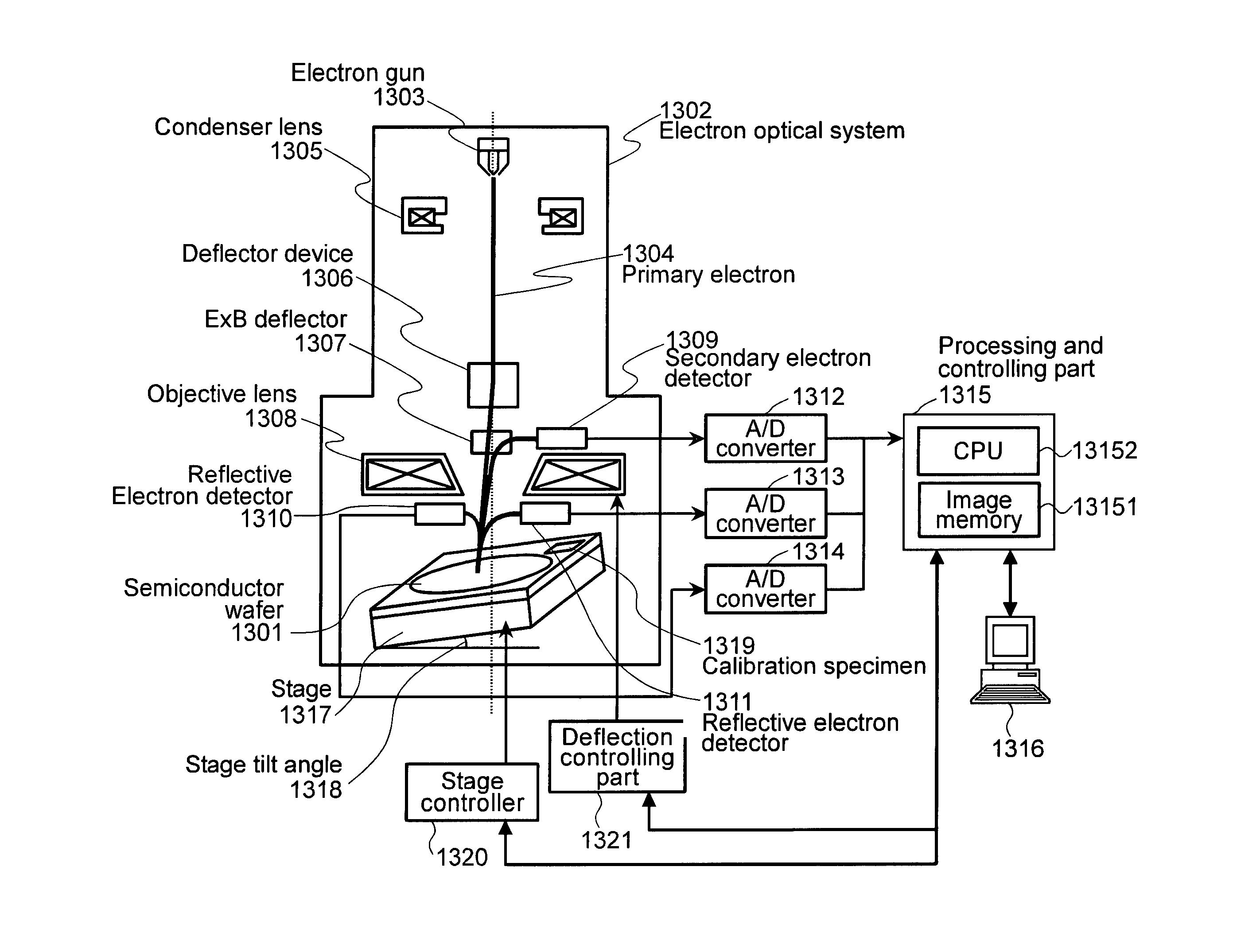
[0038]FIG. 1 shows an example of a system used to obtain and process a SEM image. An electron beam source 1303 generates an electron beam 1304. A deflector device 1306 deflects the electron beam 1304 to control the position at which the electron beam is irradiated on a specimen, such as semiconductor wafer 1301. The semiconductor wafer 1301 that is irradiated with an electron beam discharges secondary electrons and reflective electrons. The secondary electrons are detected with a secondary electron detector 1309. Meanwhile, reflective electrons are detected with the reflective electron detectors 1310 and 1311. The reflective electron detectors 1310 and 1311 are installed in different directions from each other. the secondary electrons and reflective electrons detected with the secondary electron detector 1309 and the reflective electron detectors 1310 and 1311 are...


PUM

PropertyMeasurementUnit
diametersaaaaaaaaaa
tilt angleaaaaaaaaaa

Abstract

It is predicted that an observational direction (or an incident direction of an electron beam) in an observed image actually obtained has some errors compared to a set value. The error portion affects the analysis of the observed image later. Therefore, a convergent electron beam is irradiated on a specimen with a known shape, electrons discharged from the specimen surface are detected, an image of the electron is obtained, an incident direction of the convergent electron beam is estimated based on a geometric deformation on an image of the specimen with a known shape, and a 3D shape or a shape of a cross section of a specimen to be observed from a SEM image of the specimen to be observed is obtained by use of the information of the incident direction of the estimated convergent electron beam.

Description

BACKGROUND OF THE INVENTION[0001]The present invention relates to a method and it's a device used to observe a specimen using a SEM (Scanning Electron Microscope) in the observance or measurement of a semiconductor wafer, etc in a process of semiconductor manufacture.[0002]It is getting harder to control front-end semiconductor processing as a result of the increasing miniaturization of semiconductors. Subtle changes in pattern shapes, such as corner radiuses, as well as the heights, line widths, and sidewall gradient angles of the patterns of the semiconductors, make a significant impact on the electrical characteristics of semiconductor patterns. Therefore, a technology to detect the changes in a process and control a process by measuring the dimensions or shapes of a semiconductor during manufacture is needed. A technology to estimate a 3D profile from the observations of sidewalls or images obtained by an SEM (referred to as an “SEM image” hereinafter) of a semiconductor pattern...

Claims


Application Information

Patent Timeline
Patent Type & Authority Patents(United States)
IPC IPC(8): G01N23/00G01B11/14G01B15/04G01N23/225H01J37/28
CPCG01B15/04G01N23/2251H01J37/28H01J2237/2814H01J2237/226
Inventor MIYAMOTO, ATSUSHITANAKA, MAKIMOROKUMA, HIDETOSHI
Owner HITACHI HIGH-TECH CORP
Why Eureka
Try Eureka