Active method and system of establishing electrical contact

a technology of active method and system, applied in the field of electric contacts, can solve the problems of affecting the electrical contact between the surface and the non-permanent bonding, and causing surface finish damage. to contribute to the contamination of the backside,

Inactive Publication Date: 2007-01-23
VARIAN SEMICON EQUIP ASSOC INC
View PDF6 Cites 4 Cited by
  • Summary
  • Abstract
  • Description
  • Claims
  • Application Information

AI Technical Summary

Benefits of technology

[0008]According to the methods and systems described herein, a system for electrically contacting a semiconductor wafer during implanting of the wafer can comprise one or more pairs of closely spaced contacts located adjacent the semiconductor wafer and a driving circuit connected to the contacts to provide a discharge from one contact to the semiconductor wafer and from the semiconductor wafer to the other contact of each pair of contacts. The contacts may have sharp or rounded points, or the contacts may be the inner and outer conductors of a coaxial cable. The contacts may be separated from the semiconductor wafer by a gap distance that is less than the least separation distance between the contacts. In one embodiment, the rounded points of the contacts may contact insulating surface layers on the semiconductor wafer and the discharge may pass through the insulating layer to a conduction inner portion of the semiconductor wafer.

Problems solved by technology

Making good electrical contact between surfaces that are not permanently bonded may present challenges.
The points can induce surface finish damage and can contribute to backside contamination through the introduction of foreign particles.
Also, the impedance of the resulting contacts may not be as low as may be desirable for some applications, such as such as high beam current implantations, pulsed plasma deposition processes or other processes during which maintaining close control of the potential of the wafer may be critical, even as large and / or rapidly changing currents may need to be transferred.
These standard approaches to making low-impedance electrical contact to materials can involve methods that may be undesirable or unacceptable for semiconductor processing, such as the use of large contact forces and the use of liquid, paste or gelled electronic or electrolytic conducting materials to improve contact.
Also, the use of sharply pointed contact probes may involve at least local damage at the point of contact and the so-called “spreading resistance” can limit the conductance of the contact.
While Ohmic electronic conduction is highly linear, making electrical contact can often involve highly non-linear processes due to surface insulating and semi-insulating layers and the difficulty in establishing a direct metallurgical bond between two conductors that may be brought transiently into contact.
However, improvements to electrical contacting or grounding contacts may be subject to various constraints and issues.
Material compatibility may be a concern in that grounding structures may be a source of material contamination.

Method used


Image

  • Active method and system of establishing electrical contact
  • Active method and system of establishing electrical contact
  • Active method and system of establishing electrical contact

Examples


Embodiment Construction

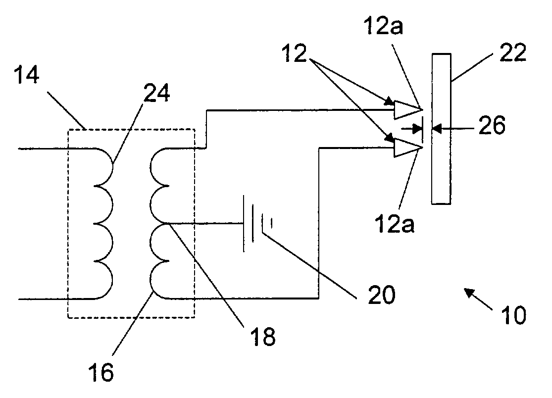
[0020]Referring now to FIG. 1, there can be shown a partial schematic diagram of a circuit 10 that can provide low impedance electrical contacting, while avoiding or reducing surface finish damage created by the electrical contacting means and reducing the introduction of foreign particles generated by the electrical contacting means. While grounding may be one of the more common purposes for electrical contacting, the devices and methods disclosed herein can be useful for a variety of electrical contacting for a variety of intended purposes. Generally, electrical excitation can be used to electrically bridge from conductor to conductor without necessarily having the conductors mechanically or physically contact one another and / or without necessarily causing permanent damage.

[0021]The electrical excitation, or discharge, may be classified as an arc, spark, corona or glow, though the classifications can overlap. The distinguishing features between the classifications may be in the co...


PUM

PropertyMeasurementUnit
conductiveaaaaaaaaaa
gap distanceaaaaaaaaaa
refractoryaaaaaaaaaa

Abstract

A system for electrically contacting a semiconductor wafer during implanting of the wafer includes one or more pairs of closely spaced contacts located adjacent the semiconductor wafer and a driving circuit connected to the contacts to provide a discharge from one contact to the semiconductor wafer and from the semiconductor wafer to the other contact of each pair of contacts. The contacts can be spaced apart from the wafer and the tips of the contacts closest to the wafer may have sharp points to aid in the establishment of corona at lower drive voltages. Alternately, the contacts may be rounded and may contact the wafer. The driving circuit may be adapted from a pulsed discharge circuit, such as a Kettering ignition circuit, a capacitance discharge ignition circuit, or a blocking oscillator circuit. Alternately, the driving circuit may be adapted from a continuous discharge circuit, such as a Tesla coil circuit.

Description

RELATED APPLICATIONS[0001]There are no related applications.FIELD[0002]The methods and systems relate to electrical contacts, and more particularly to the use of electrical excitation to create electrical contacts.BACKGROUND[0003]Making good electrical contact between surfaces that are not permanently bonded may present challenges. As an example, in the semiconductor processing industry, contacts may need to be applied to the silicon wafers for grounding the wafers during the implantation process, for removing beam induced charge during implantation and / or for controlling the potential of the wafer during the implantation process. Similar situations may exist in other industries, e.g., in the design of switches, relays, plugs and sockets. Typical solutions can involve mechanical deformations, e.g., wiping, piercing, scouring and / or polishing, in order to provide clean conductor-to-conductor junctions. Sometimes liquids, gels and / or pastes may be used to enhance the conductance of th...

Claims


Application Information

Patent Timeline
Patent Type & Authority Patents(United States)
IPC IPC(8): G05F3/04H01F29/02
CPCH01J37/32412H01J37/20H01F29/02H01J2237/0041H01L21/02
Inventor RHOADS, KEVIN G.
Owner VARIAN SEMICON EQUIP ASSOC INC
Why Eureka
Try Eureka