Optical deflection device
a technology of optical deflection and optical deflection, which is applied in the direction of reflex reflectors, instruments, record information storage, etc., can solve the problems of difficult to maintain stability of beams, low response speed, and torsion beam digital micro-mirror devices, so as to reduce the density of mirrors, prevent the reduction of reflection efficiency, and rotate smoothly
- Summary
- Abstract
- Description
- Claims
- Application Information
AI Technical Summary
Benefits of technology
Problems solved by technology
Method used
Image


Examples
first embodiment
[0047
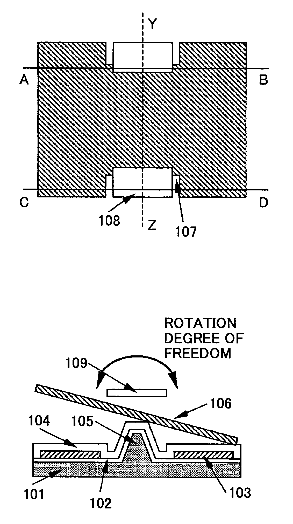
[0048]FIGS. 1A through 1F are views schematically showing a first example of a configuration of an optical deflection device according to an embodiment of the present invention, where, FIG. 1A is a plan view of the optical deflection device, FIG. 1B is a plan view of electrodes with a mirror being removed, FIG. 1C is a cross-sectional view of the optical deflection device along the line AB in FIG. 1A, FIG. 1D is a plan view of a mirror, FIG. 1E is a cross-sectional view of the optical deflection device along the line YZ in FIG. 1A, and FIG. 1F is a cross-sectional view of the optical deflection device along the line CD in FIG. 1A.
[0049]As illustrated in FIG. 1C, a ridge 105 acting as a fulcrum member is formed on a silicon substrate 101, and both are insulated by an oxide film 102. A number of electrodes 103, for example, four electrodes 103 (also referring to FIG. 1B), are provided, and are covered by an insulating film such as an oxide film 104.
[0050]The ridge 105 functions a...
second embodiment
[0071
[0072]Below, a typical method of forming notches in the mirror 106 is described with reference to FIGS. 5A through 5E, FIGS. 6A through 6E, FIGS. 7A through 7F, and FIG. 8. In the following description, it is assumed that the mirror is a 20 μm square, and the inclination angle of the mirror is 15°.
[0073]FIGS. 5A through 5D are cross-sectional views showing steps of forming the optical deflection device having the notches 107 in the mirror 106 according to a second embodiment of the present invention, where FIG. 5E is a plan view corresponding to FIG. 5D, which shows the cross-sectional view along a line AB in FIG. 5E.
[0074]As illustrated in FIG. 5A, a mask is formed on a substrate 101 (for example, a silicon wafer) by photolithography with an organic resist and a photo mask having grade levels. Afterwards, the silicon substrate 101 is etched to a thickness of 2.6 μm by RIE (Reactive Ion Etching) with a mixed gas of SF6 and O2, thereby, forming the ridge 105. Then, thermal oxida...
third embodiment
[0086
[0087]Below, a typical method of forming the ring mechanism for loosely fixing the mirror 106 is described with reference to FIGS. 9A through 9E, FIGS. 10A through 10E, FIGS. 11A through 11F, and FIG. 12. In the following description, it is assumed that the mirror is a 20 μm square, rectangular openings in the mirror 106 are 4 μm along the axle direction and 5 μm in the rotation direction, and the inclination angle of the mirror is 15°.
[0088]FIGS. 9A through 9D are cross-sectional views showing steps of forming the optical deflection device having the openings 122 and the ring mechanism on the mirror 106 according to a third embodiment of the present invention, where FIG. 9E is a plan view corresponding to FIG. 9D, which shows the cross-sectional view along a line AB in FIG. 9E.
[0089]As illustrated in FIG. 9A, a mask is formed on a substrate 101 (for example, a silicon wafer) by photolithography with an organic resist and a photo mask having grade levels. Afterwards, the silico...
PUM
| Property | Measurement | Unit |
|---|---|---|
| inclination angle | aaaaa | aaaaa |
| thickness | aaaaa | aaaaa |
| thickness | aaaaa | aaaaa |
Abstract
Description
Claims
Application Information