Global bit line restore timing scheme and circuit
a bit line restoration and timing scheme technology, applied in the field ofdomino static random access memory, can solve problems such as difficulty in line up the bit line restore puls
- Summary
- Abstract
- Description
- Claims
- Application Information
AI Technical Summary
Benefits of technology
Problems solved by technology
Method used
Image
Examples
Embodiment Construction
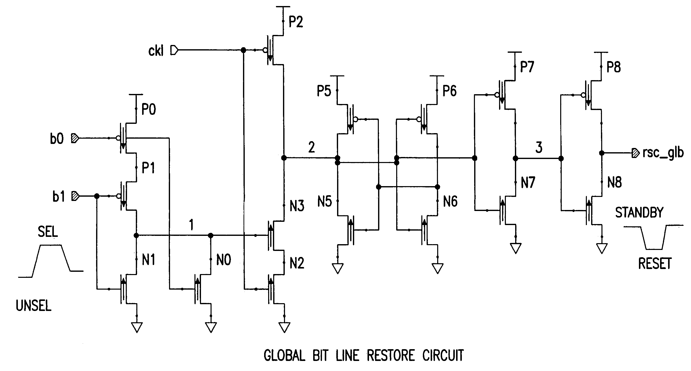
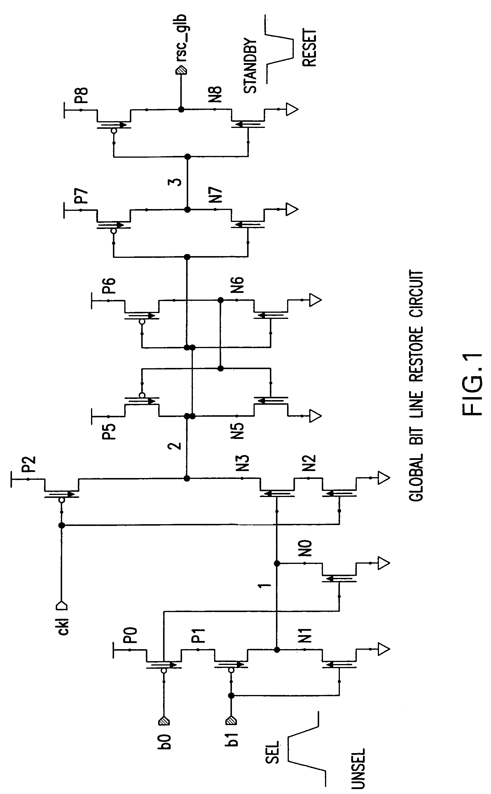
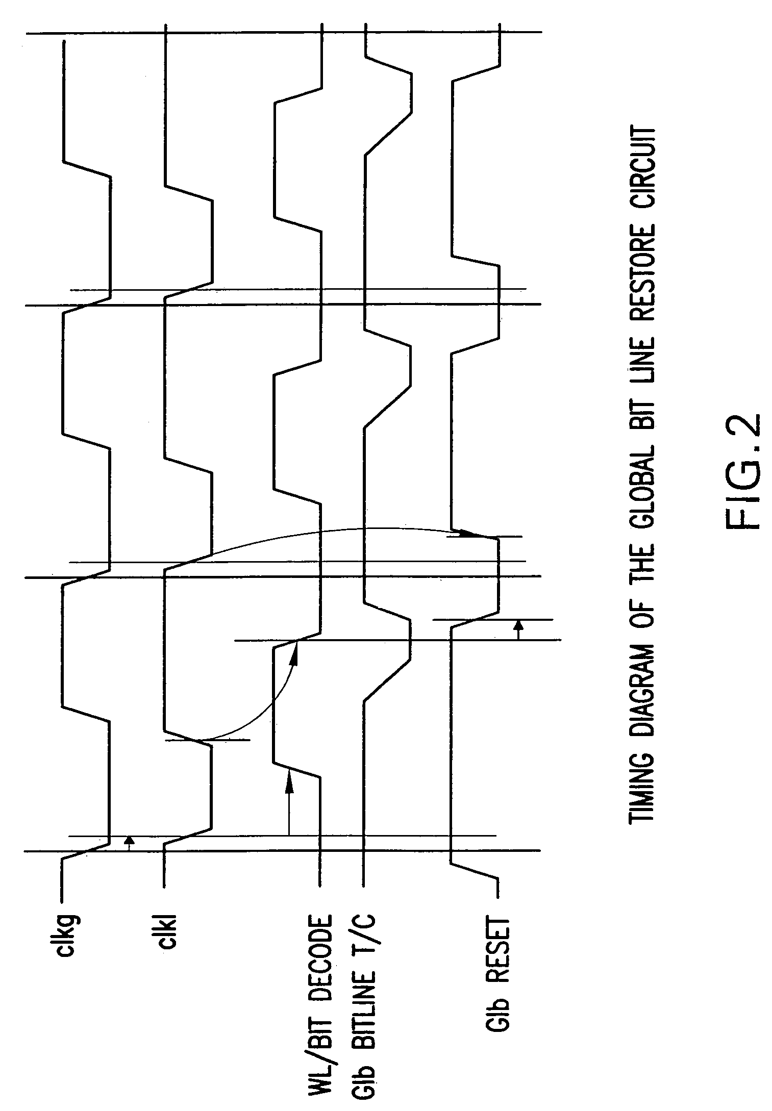
[0015]Referring now to FIGS. 1 and 2 of the drawings, b0 and b1 are the bit decode signal lines for a 1-out-of-2 bit decode system. For a 1-out-of-4 bit decode, there will be 4 decode lines b0–b3. The bit decode outputs, also referred to as Global-Column-Select in the above referenced copending patent applications, are fed to the global bit select circuits to perform the column select function. They should not be confused with the global bit lines, which are the read and write bit line pairs in the global bit select circuits. The clk1 is the active low local array clock signal that enables the bit and word select lines. In standby mode, ckl is high, turning on nfet transistor N2. The bit decode lines b0 and b1 are low, and node 1 is pulled up, turning on transistor N3. This pulls down node 2, thus giving a ‘low’ at global bit line restore output rsc_glb, which restores the global bit lines from the global bit select circuits. In active mode, at the beginning of a read or write cycle...
PUM
 Abstract
Description
Claims
Application Information


