Semiconductor test system

a test system and semiconductor technology, applied in the field of semiconductor test systems, can solve the problems of increasing the sampling rate and the circuit size of the digitizer, and achieve the effects of high speed, high resolution and high performance of the digitizer

Active Publication Date: 2007-02-06
ADVANTEST CORP
View PDF10 Cites 30 Cited by
  • Summary
  • Abstract
  • Description
  • Claims
  • Application Information

AI Technical Summary

Benefits of technology

[0025]According to the present invention, an input analog signal which repeats the same wave form in the time period T by M cycles is sampled by the digitizer for the M cycles wherein a phase of the sampling clock is shifted by a predetermined amount ΔP (delta phase) for each cycle. As a result, the data obtained in the AD conversion process of the present invention shows resolution M times...

Problems solved by technology

As a consequence, in the conventional technology involving the interleave method, there is a pro...

Method used


Image

  • Semiconductor test system
  • Semiconductor test system
  • Semiconductor test system

Examples


Embodiment Construction

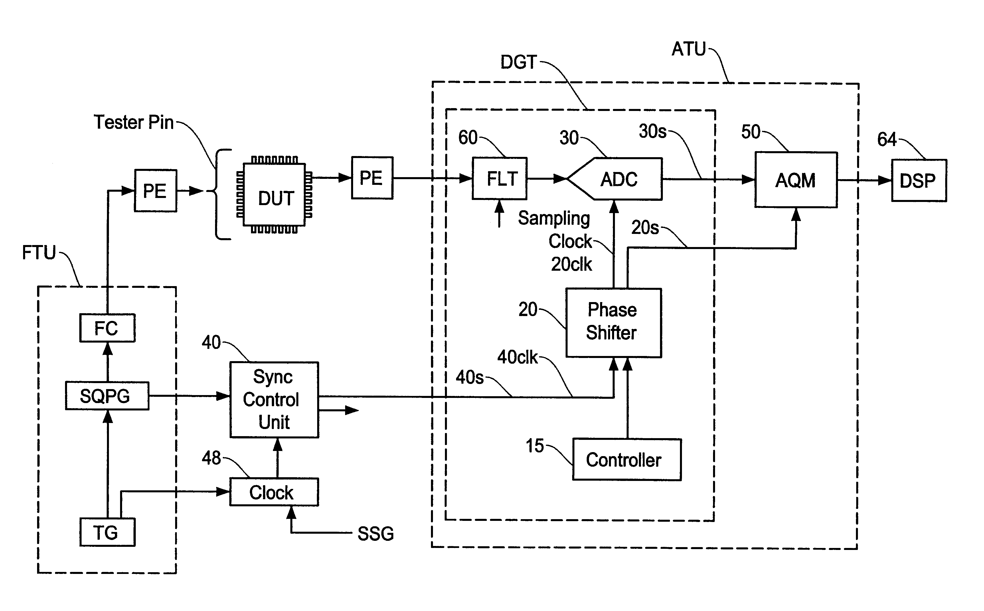
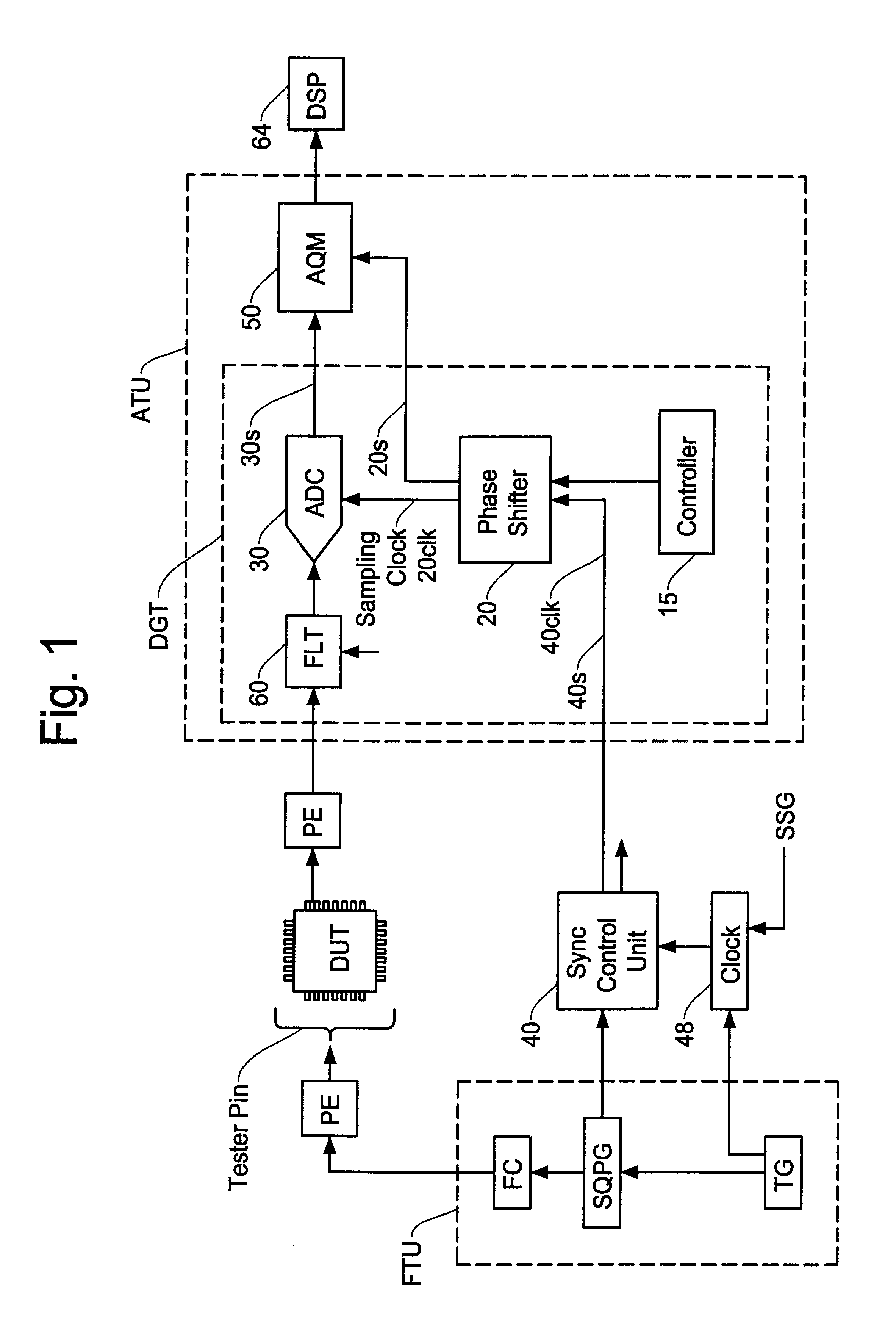
[0036]An embodiment of the present invention is shown in FIGS. 1-3. An example of structure of the mixed signal semiconductor test system of the present invention is shown in a block diagram of FIG. 1 in which an emphasis is placed on a digitizer DGT. In the present invention, to increase the sampling rate of the digitizer, a phase of the sampling clock signal is shifted by a predetermined degree for each cycle of an input analog signal.

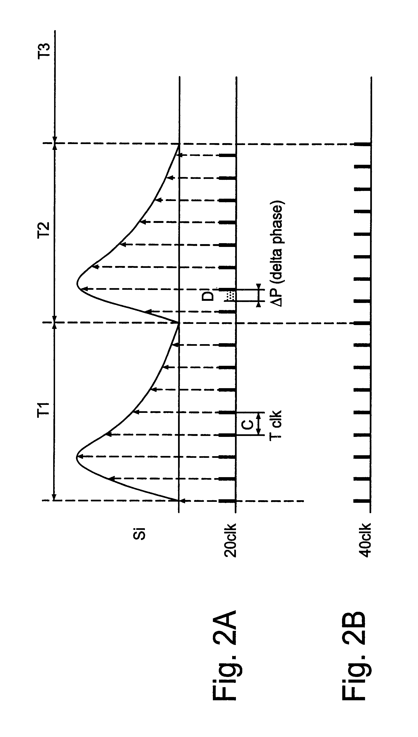
[0037]This invention is based on the fact that, almost always, a wave form of a time period T shown in FIGS. 2A and 2B in an output analog signal of a device under test (DUT) is repeated by a plurality of times. This is because, in a mixed signal test system, clock and other signals can be freely supplied to the DUT from the test system so that the repetition rate of the output analog signal of the DUT can be controlled or predictable by the test system. Thus, in the present invention, a digitizer DGT in the mixed signal test system includes only one...


PUM


Abstract

A mixed signal test system for testing a semiconductor device having both an analog function and a digital function achieves improved resolution and low cost. The test system is formed of a functional test unit for testing a digital function of a device under test (DUT), an analog test unit (ATU) for testing an analog function of the DUT, and a synchronous control unit for synchronizing operations between the functional test unit and the analog test unit. The analog test unit includes a digitizer for converting an analog output of the DUT into a digital signal, and an acquisition memory for storing the digital signal from the digitizer in specified addresses. The wave form of the analog output is repeated by a plurality of cycles and a sampling clock for the digitizer is phase shifted by a predetermined amount for each cycle.

Description

FIELD OF THE INVENTION[0001]This invention relates to a semiconductor test system for testing semiconductor devices such as mixed signal ICs and LSIs, and more particularly, to a semiconductor test system having a digitizer for continuously performing AD conversion of an analog signal from a device under test where an equivalent sampling frequency in the AD conversion is substantially increased.BACKGROUND OF THE INVENTION[0002]In testing semiconductor devices such as ICs and LSIs by a semiconductor test system, such as an IC tester, a semiconductor IC device to be tested is provided with test signals produced by an IC tester at its appropriate tester pins (channels) at predetermined test timings. The IC tester receives output signals from the IC device under test generated in response to the test signals. The output signals are strobed by strobe signals with predetermined timings to be compared with expected data to determine whether or not the IC device properly performs the intend...

Claims


Application Information

Patent Timeline
IPC IPC(8): G01R13/14G01R31/02G01R31/26G01R31/3193
CPCG01R31/31935
Inventor ASAMI, KOJI
Owner ADVANTEST CORP
Why Eureka
Try Eureka