Method and apparatus for automated circuit design

Active Publication Date: 2007-02-13
SYNOPSYS INC
View PDF8 Cites 43 Cited by
  • Summary
  • Abstract
  • Description
  • Claims
  • Application Information

AI Technical Summary

Benefits of technology

[0011]In one aspect of the present invention, a method to design a circuit includes: determining likelihood of a design constraint (e.g., a timing constraint, maximum capacitance, maximum transition, maximum crosstalk) being violated in an implementation of a first circuit design (e.g., a technology specific netlist with or without a placement solution); and, modifying the first circuit design to reduce the likelihood of the design constraint being violated. In one example, the implementation of the first circuit design includes a routing solution for implementing the first circuit design; and, the first circuit is modified through sizing an instance of a logic element, buffering a signal, load shielding for a signal, sizing a weakest driver of a logic element or other operations. In one example, the design constraint includes a timing constraint (e.g., worst negative slack of the circuit, a slack for an instance of a logic element in the first circuit design, a delay on a path in the first circuit design, a total negative slack of the circuit, or others). A total negative slack of a circuit is the sum of all negative slack at all endpoints of a circuit. An endpoint of a circuit is a point in the circuit where a path ends. In one example, modifying the first circuit design includes selecting an instance of a logic element for modification according to sensitivity of a para

Problems solved by technology

Since all logic elements corresponding to a net with a certain fanout are assumed to have the same wire delay, the estimated delay information is not very accurate.
Due to the error in the delay estimator in logic synthesis, a solution appears to be valid during logic synthesis may be found invalid after the placement and routing operation.
However, in place optimizations can provide only limited improvements.
When the in place optimization cannot adjust the solution to meet the timing constraint, adju

Method used


Image

  • Method and apparatus for automated circuit design
  • Method and apparatus for automated circuit design
  • Method and apparatus for automated circuit design

Examples


Embodiment Construction

[0020]The following description and drawings are illustrative of the invention and are not to be construed as limiting the invention. Numerous specific details are described to provide a thorough understanding of the present invention. However, in certain instances, well known or conventional details are not described in order to avoid obscuring the description of the present invention. References to one or an embodiment in the present disclosure are not necessary references to the same embodiment; and, such references means at least one.

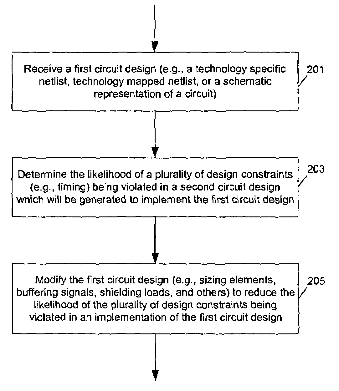
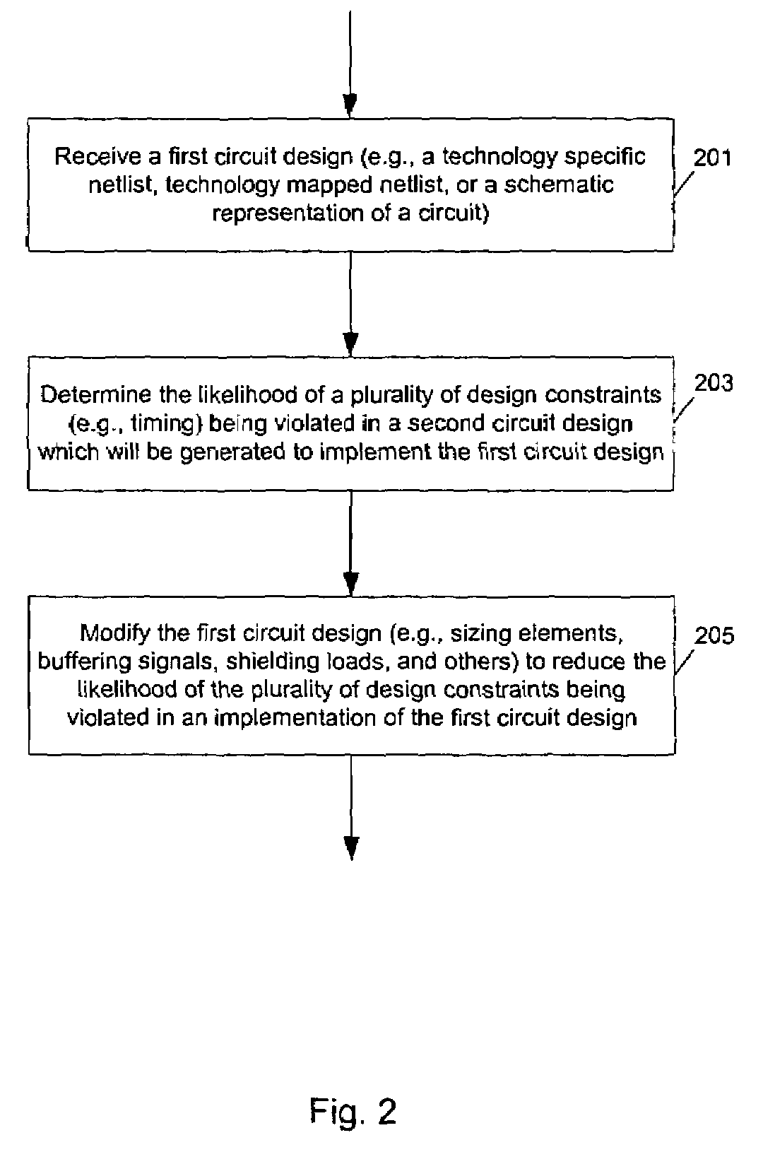
[0021]At least one embodiment of the present invention seeks to optimize a circuit design (e.g., a synthesis solution of a technology specific design) so that the likelihood of design constraints being violated in an implementation of the circuit design is reduced (e.g., after placement and routing). In one embodiment, a minimum set of instances is selected for transformation to decrease the probability that they will be involved in the violation of...


PUM


Abstract

Methods and apparatuses to automatically modify a circuit design (e.g., a synthesis solution) according to the sensitivity in design parameters with respect to the possible deviation in the subsequent implementation (e.g., placement and routing) of the circuit. In one aspect of the present invention, a method to design a circuit includes: determining likelihood of a design constraint being violated in an implementation of a first circuit design (e.g., a technology specific netlist with or without a placement solution); and, modifying the first circuit design to reduce the likelihood of the design constraint being violated. In one example, the implementation of the first circuit design includes a routing solution for implementing the first circuit design; and, the first circuit is modified through sizing an instance of a logic element, buffering a signal, load shielding for a signal, or other operations.

Description

[0001]The present invention claims the benefit of the filing date of provisional application Ser. No. 60 / 475,059, filed May 30, 2003 and entitled “Method and Apparatus for Automated Circuit Design”, by the inventors Champaka Ramachandran, Andrew Crews and Kenneth S. McElvain, which is hereby incorporated herein by reference.FIELD OF THE INVENTION[0002]The invention relates to automated circuit design, and more particularly to the automated optimization of the design of a circuit before performing a detailed design layout.BACKGROUND[0003]For the design of digital circuits (e.g., on the scale of Very Large Scale Integration (VLSI) technology), designers often employ computer-aided techniques. Standard languages such as Hardware Description Languages (HDLs) have been developed to describe digital circuits to aid in the design and simulation of complex digital circuits. Several hardware description languages, such as VHDL and Verilog, have evolved as industry standards. VHDL and Verilog...

Claims


Application Information

Patent Timeline
IPC IPC(8): G06F17/50
CPCG06F17/5031G06F17/505G06F17/5072G06F2217/84G06F2217/10G06F2111/08G06F30/3312G06F30/327G06F2119/12G06F30/392
Inventor RAMACHANDRAN, CHAMPAKACREWS, ANDREWMCELVAIN, KENNETH S.
Owner SYNOPSYS INC
Why Eureka
Try Eureka