Display device having a display drive section

a display drive and display device technology, applied in the field of display devices, can solve the problems of increasing the amount of useless data transmission, increasing the power consumption, and the inability to achieve the reduction of power consumption, so as to improve the reduction of consumption power, prevent noise superposition, and reduce the cross-over of interconnections

Inactive Publication Date: 2007-02-20
SHENZHEN CHINA STAR OPTOELECTRONICS TECH CO LTD
View PDF24 Cites 77 Cited by
  • Summary
  • Abstract
  • Description
  • Claims
  • Application Information

AI Technical Summary

Benefits of technology

[0050]In this invention, crossover of interconnections is decreased to improve reduction in consumption power. Also, in order to prevent noise superposition due to the effect of switchi...

Problems solved by technology

Due to this, there is an increase in useless data transmission amount and hence ...

Method used


Image

  • Display device having a display drive section
  • Display device having a display drive section
  • Display device having a display drive section

Examples


embodiment 1

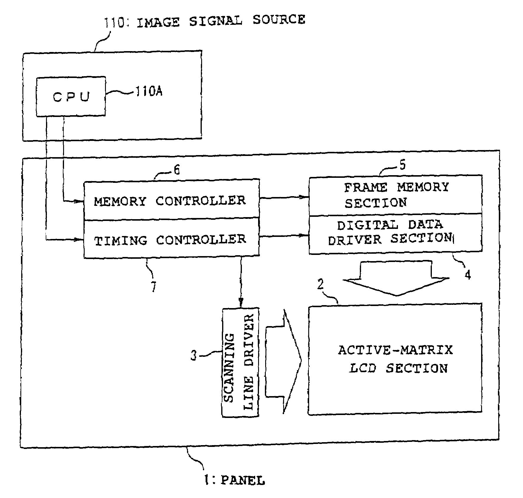
[0078]FIG. 1 is a block diagram showing a concept of a system including a display device according to Embodiment 1 of the present invention. FIG. 1 represents a concept called system-on-panel (SOP). SOP is the concept to form a peripheral circuit for display or the like over a glass substrate, and moreover to integrally form TFTs or the like together with the peripheral circuit by the use of poly-silicon or the like without using chips of ICs or the like. Due to this, the panel can be directly coupled to the CPU while achieving low cost, high reliability and space saving.

[0079]In FIG. 1, an image signal source 110 is configured by a CPU 110A to transmit display data. Herein, the display data is transmitted with image signals as digital data, similarly to the conventional configuration shown in FIG. 11. If the image signal is digital data, D / A conversion is not required on the side of a panel 1, correspondingly achieving the reduction in size and power consumption. Meanwhile, the pan...

embodiment 2

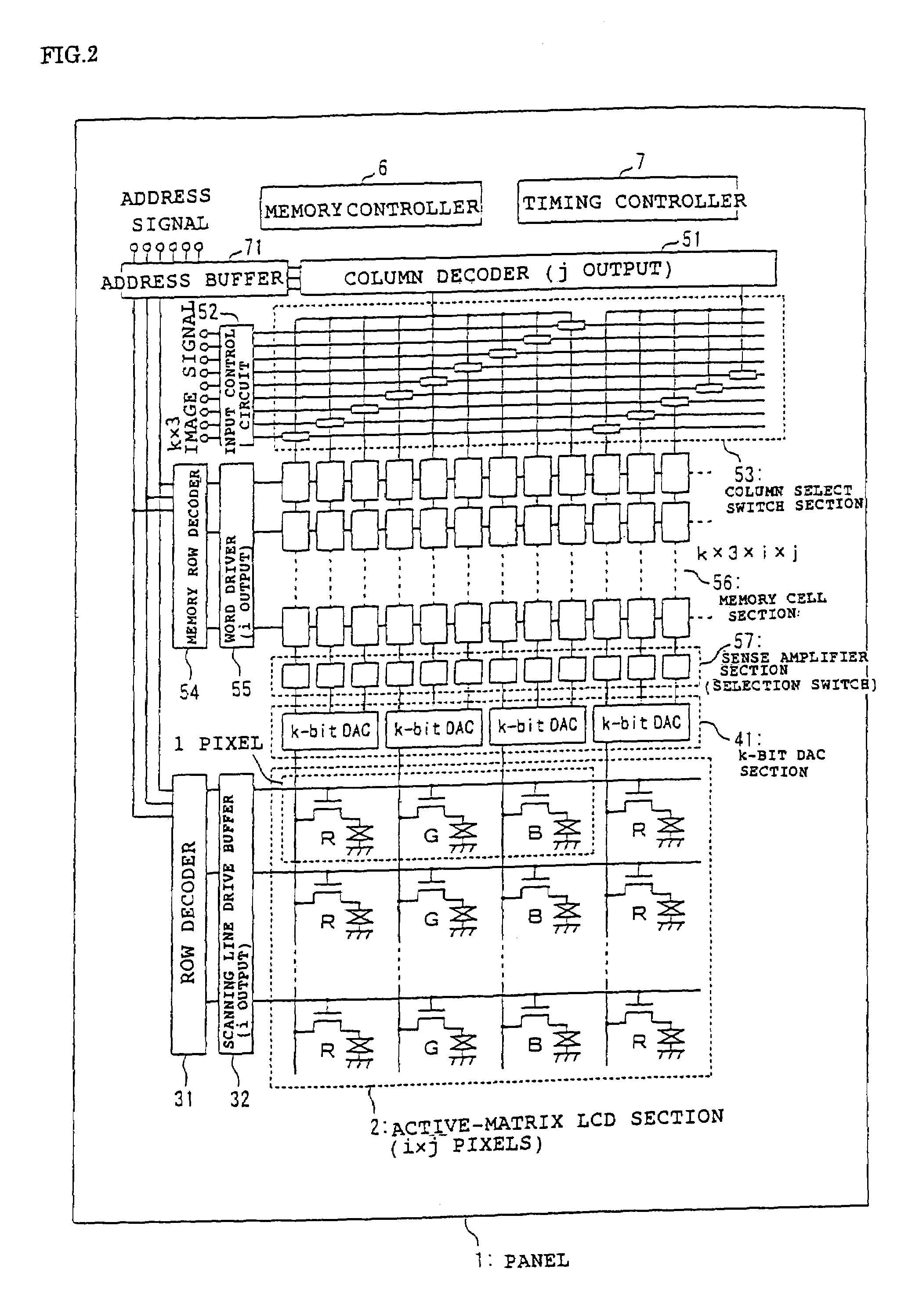
[0104]FIG. 3 is a figure showing in detail a panel 1A according to a second embodiment of the invention. The panel 1A of FIG. 3 differs from the panel 1 of FIG. 2 in that address signals are independently inputted to the row decoder 31 and the memory row decoder 54. Due to this, it is possible to make the timing of storage different from the timing of display operations. The drive frequency is higher than that of storage and display operations in simultaneous timing. However, various forms of driving is feasible, e.g., address data is transmitted to the memory row decoder 54 in certain timing to make storage operation, and then address data is transmitted to the row decoder 31 in the next timing to make display.

[0105]As above, according to the second embodiment, because address signals are independently inputted respectively to the row decoder 31 and the memory row decoder 54, it is possible to enhance the freedom for selecting a drive method.

embodiment 3

[0106]FIG. 4 is a figure showing in detail a panel 1B according to a third embodiment of the invention. The panel 1B of FIG. 4 differs from the panel 1 of FIG. 2 in that a scanning line-select-control signal line and a word line-select-control signal line are respectively laid from the address buffer 71 to the row decoder 31A and the memory row decoder 54A, to transmit a scanning line-select-control signal and a word-line-select-control signal. The same address signal is inputted to the row decoder 31A and the memory row decoder 54A. However, the row decoder 31A is allowed to select a scanning line only during the period that a scanning line-select-control signal is on. Also, the memory row decoder 54A similarly is allowed to select a word line only during the period that a word-line-select-control signal is on. Consequently, storage and display operations can be made in different timing depending upon control of on-off of these signals.

[0107]As above, according to the third embodim...


PUM


Abstract

The invention provides a display device having, integrated on a substrate and integrally formed therewith, an active-matrix LCD section having a plurality of scanning lines and a plurality of data lines formed in a grating form corresponding to dots, and active elements according to the respective intersections to perform display control using a liquid crystal by driving the scanning lines and the data lines. The display device further including a row decoder for selecting the scanning lines, a memory cell section having memory cells that are in the number capable of storing an image signal for display control of dots in at least one row of a display drive section and allocated corresponding to the length in the row direction of the display drive section. The display device further having a column decoder section for selecting a memory cell to be stored with an inputted image signal, a column selection switch section switching on the basis of a selection by the column decoder section 51 and the image signal and storing the image signal to the memory cell selected, and a k-bit DAC section 41 for driving a data line on the basis of the image signal stored in the memory cell section.

Description

TECHNICAL FIELD[0001]The present invention relates to display devices. More particularly, the invention relates to a drive circuit or the like to make display on a liquid crystal display (LCD: Liquid Crystal Display) or an organic EL display (OELD: Organic Electro Luminescent Display).BACKGROUND OF THE INVENTION[0002]Recently, display devices using liquid crystal (hereinafter, referred to as display) are spreading at conspicuous pace. The display of this type is low in power consumption and improved in saving space in comparison with a CRT display. Accordingly, it is important to make use of the merits of such a display and produce a display that is lower in power consumption and improved in saving space.[0003]FIG. 11 is a block diagram of a system to implement display through a display device with a TFT display. This system is constituted with an image signal source 100 and a TFT liquid crystal display panel 101. The image signal source 100 is formed, at least, by a CPU 100A, a RAM...

Claims


Application Information

Patent Timeline
IPC IPC(8): G09G5/00G09G3/32G09G3/36
CPCG09G3/3233G09G3/3291G09G3/3648G09G3/3688G09G3/2074G09G2310/027G09G5/395G09G2300/0408G09G2300/0443G09G2300/0809G09G2300/0842G09G5/393G09G3/36
Inventor MATSUEDA, YOJIRO
Owner SHENZHEN CHINA STAR OPTOELECTRONICS TECH CO LTD
Why Eureka
Try Eureka