Method for manufacturing electro-optical device, electro-optical device, and electronic apparatus

Inactive Publication Date: 2007-02-27
SEIKO EPSON CORP
View PDF28 Cites 24 Cited by
  • Summary
  • Abstract
  • Description
  • Claims
  • Application Information

AI Technical Summary

Benefits of technology

[0036]As described above, the etching step is performed on the exposed entire surface, edges, and cut faces (side surfaces) of the substrates even in a state where the protection layer is formed. Thus, the outer surfaces of the etched portions are etched thinly to remove fine scratches or cracks. As a result, the strength of the panel is enhanced. When a wet etching is performed, t

Problems solved by technology

However, in any one of the cutting methods, small scratches or cracks are made on the edge or the cut faces of the substrate by stress in the process of cutting the substrate, and those scratches or cracks are grown by additional stress.
As a result, if a liquid crystal device is used in a mobile phone, a liquid crystal panel is broken by an impact when the mobile phone is dropped.
However, since strong acid such as hydrofluoric acid is used to

Method used


Image

  • Method for manufacturing electro-optical device, electro-optical device, and electronic apparatus
  • Method for manufacturing electro-optical device, electro-optical device, and electronic apparatus
  • Method for manufacturing electro-optical device, electro-optical device, and electronic apparatus

Examples


Example

[0088]First Embodiment

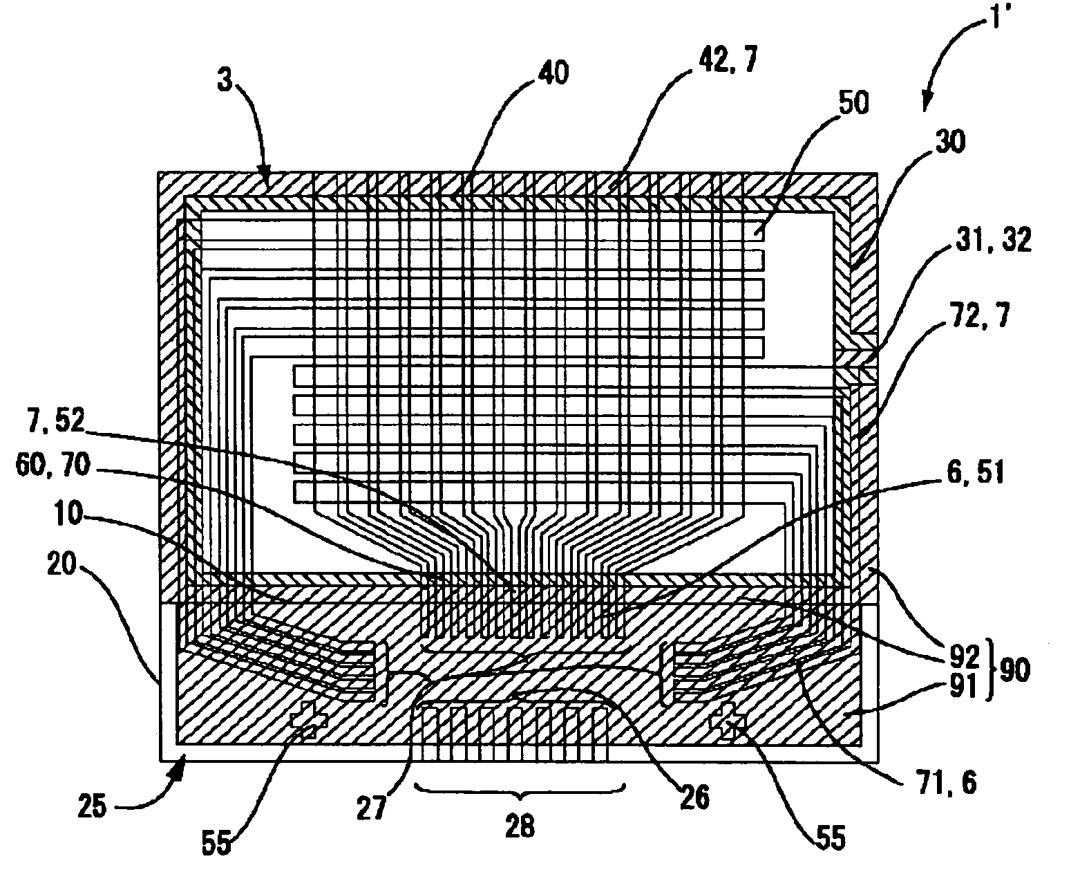
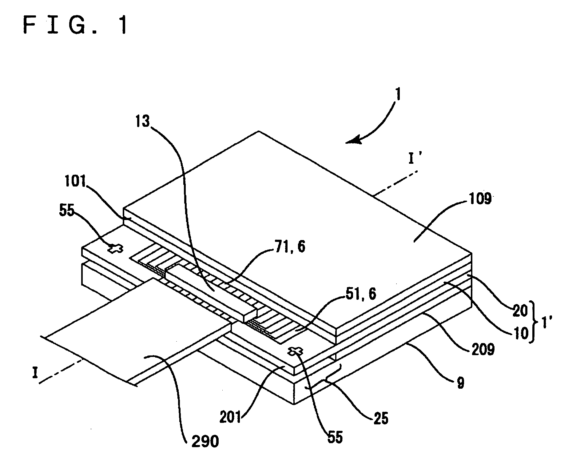
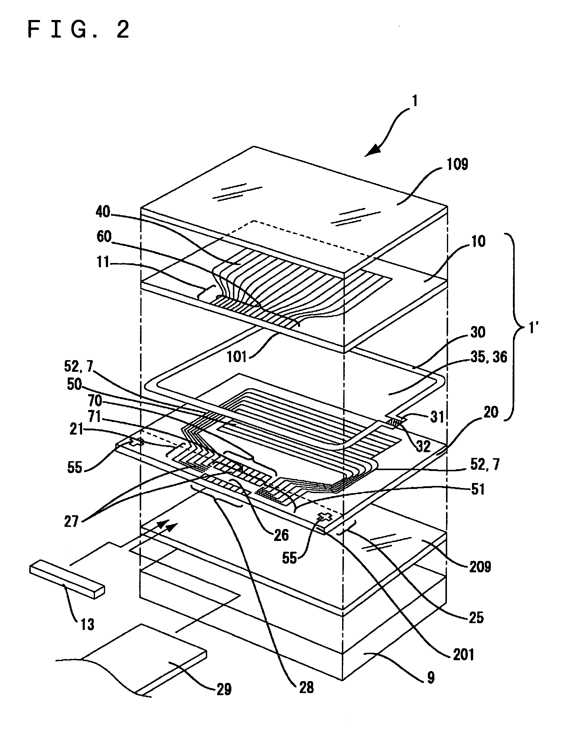
[0089]FIG. 6(A) is a diagram schematically illustrating fine scratches or cracks made on the substrate constituting the liquid panel 1′, and FIG. 6(B) is a diagram illustrating a state where the fine scratches or cracks are removed from the substrate by an etching step. FIGS. 7(A) and 7(B) are a plan view and a cross-sectional view of the liquid crystal panel during the manufacturing processes for an electro-optical device, respectively. FIGS. 8(A) and 8(B) are a plan view and a cross-sectional view showing a state where a protection layer is formed when an etching step is performed on the liquid crystal panel in the manufacturing processes of the electro-optical device, respectively. FIGS. 9(A) and 9(B) are a plan view and a cross-sectional view showing a state where a part of the protection layer remains after the etching step is performed on the liquid crystal panel in the manufacturing processes of the electro-optical device, respectively. FIGS. 10(A) to 10...

Example

[0105]Second Embodiment

[0106]The second to sixth embodiments have the same basic structures as the first embodiment. Accordingly, only the characteristic parts of the second to sixth embodiments will now be explained with reference to FIGS. 7 to 9, and the explanation of the same parts will be omitted.

[0107]In this embodiment, similar to the first embodiment, the liquid crystal panel 1′ is cut as a single product in the second break step ST34 shown in FIG. 5(E), and then the wet etching step is performed on the cut faces and edges of the first substrate 10 and the second substrate 20 of the single product liquid crystal panel 1′ before the driving IC 13 is mounted on the protruding region 25 of the single product liquid crystal panel 1′ in the IC mounting step ST35 shown in FIG. 5(F), thereby removing fine scratches or cracks from the edges and the cut faces of the substrates (the etching step ST40).

[0108]In the manufacturing process of the electro-optical device 1, fine scratches o...

Example

[0115]Third Embodiment

[0116]In this embodiment, a liquid crystal panel 1′ is cut as a single product in the second break step ST34 shown in FIG. 5(E), and then the wet etching is performed on the edges and cut faces of the first substrate 10 and the second substrate 20 of the single product liquid crystal panel 1′ before the driving IC 13 is mounted on the protruding region 25 of the single product liquid crystal panel 1′ in the IC mounting step ST35 shown in FIG. 5(F), thereby removing fine scratches or cracks from the edges and the cut faces of the substrates (etching step ST40). In the manufacturing process of an electro-optical device 1, fine scratches or cracks may be generated on the cut faces and edges of the first substrate 10 and the second substrate 20 as well as on other surfaces thereof. In order to remove such scratches and cracks, the etching step ST40 can be performed not only on the cut faces and edges of the first substrate 10 and the second substrate 20 but also on...


PUM


Abstract

A method is provided for manufacturing an electro-optical device, in which fine scratches or cracks can be removed by etching without damaging wiring, an electro-optical device, and an electronic apparatus. According to the method, a liquid crystal panel used in an electro-optical device is cut as a single product. Then, before an IC mounting step, in a state of the single product liquid crystal panel, a wet etching is performed on the cut faces and edges of the first and second substrates to remove fine scratches or cracks from the cut faces and edges of the substrates. At this time, wiring portions, IC mounting terminals, substrate mounting terminals, and alignment marks, which are formed on the protruding region, are covered with a protection layer.

Description

BACKGROUND OF THE INVENTION[0001]1. Technical Field of the Invention[0002]The present invention generally relates to a method for manufacturing an electro-optical device including an electro-optical panel having a pair of substrates, which have a predetermined size and are bonded to be opposite to each other, an electro-optical device manufactured by the method, and an electronic apparatus using the electro-optical device. More specifically, the present invention relates to a process for preventing the substrates from being cracked in the state of an electro-optical panel.[0003]2. Description of the Related Art[0004]Electro-optical devices, such as liquid crystal devices, LED (Light-Emitting Diode) display devices including organic electro-luminescence display devices, plasma display devices, FED (Field Emission display) devices, electrophoresis display devices, and DMDs (Digital Micro-mirror Devices), have a panel structure in which a pair of glass substrates, on which driving elec...

Claims


Application Information

Patent Timeline
IPC IPC(8): B29D11/00G02F1/13
CPCG02F1/13452G02F1/133351G02F2201/50G02F2001/133302G02F1/133302G02F1/13
Inventor MURAI, HIDETOSHIHANAKAWA, MANABU
Owner SEIKO EPSON CORP
Why Eureka
Try Eureka