

Data signal line drive circuit, drive circuit, image display device incorporating the same, and electronic apparatus using the same
a drive circuit and drive circuit technology, applied in the direction of static indicating devices, instruments, television systems, etc., can solve the problems of reducing power consumption, affecting the life of the battery, and limited video display capability, so as to reduce the total power consumption of the electronic apparatus and improve the display quality of the output device.
- Summary
- Abstract
- Description
- Claims
- Application Information
AI Technical Summary
Benefits of technology
Problems solved by technology
Method used
Image

Examples
embodiment 1
[0207]Referring to FIG. 1 to FIG. 92, the following will describe an embodiment in accordance with the present invention.
[0208]An image display device of the present embodiment includes a plurality of drive circuits which is switchable to the most suitable display mode and format depending on the kind of video data and environmental conditions to achieve both high display quality and low power consumption and which operate simultaneously to produce a superimposed display of a plurality of sets of image data.
[0209]In the present embodiment, an active matrix liquid crystal display device will be described as an example of image display devices related to the technologies of interest in the present invention. However, the present invention is not limited to the example and is equally applicable to image display devices of other types.
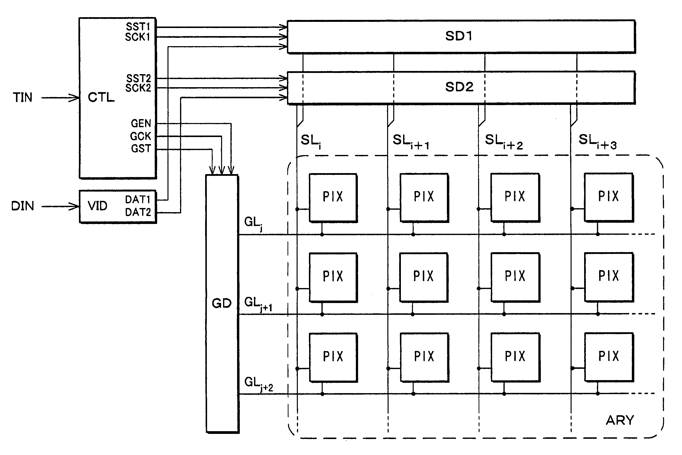
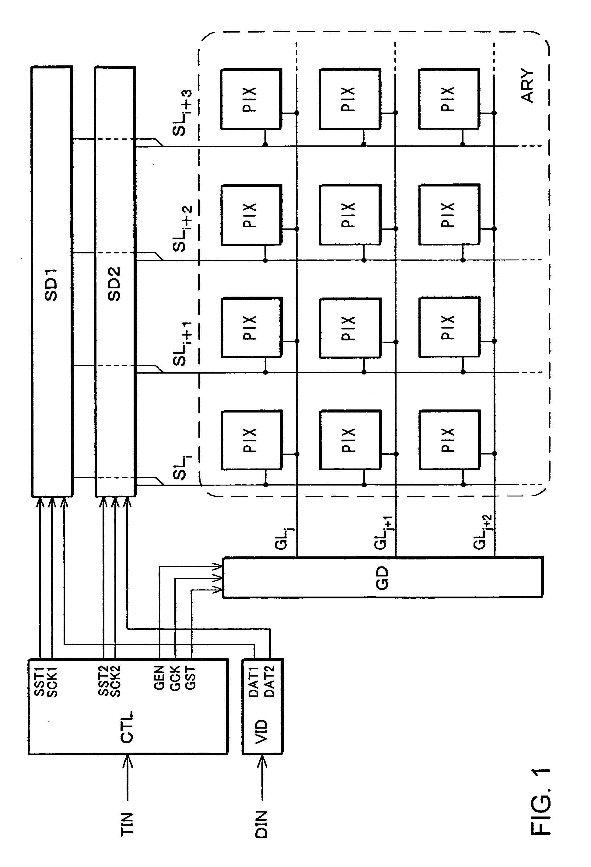
[0210]FIG. 1 to FIG. 7 are block diagrams showing, as an example, a configuration of an image display device in accordance with the present invention.
[021...
embodiment 2
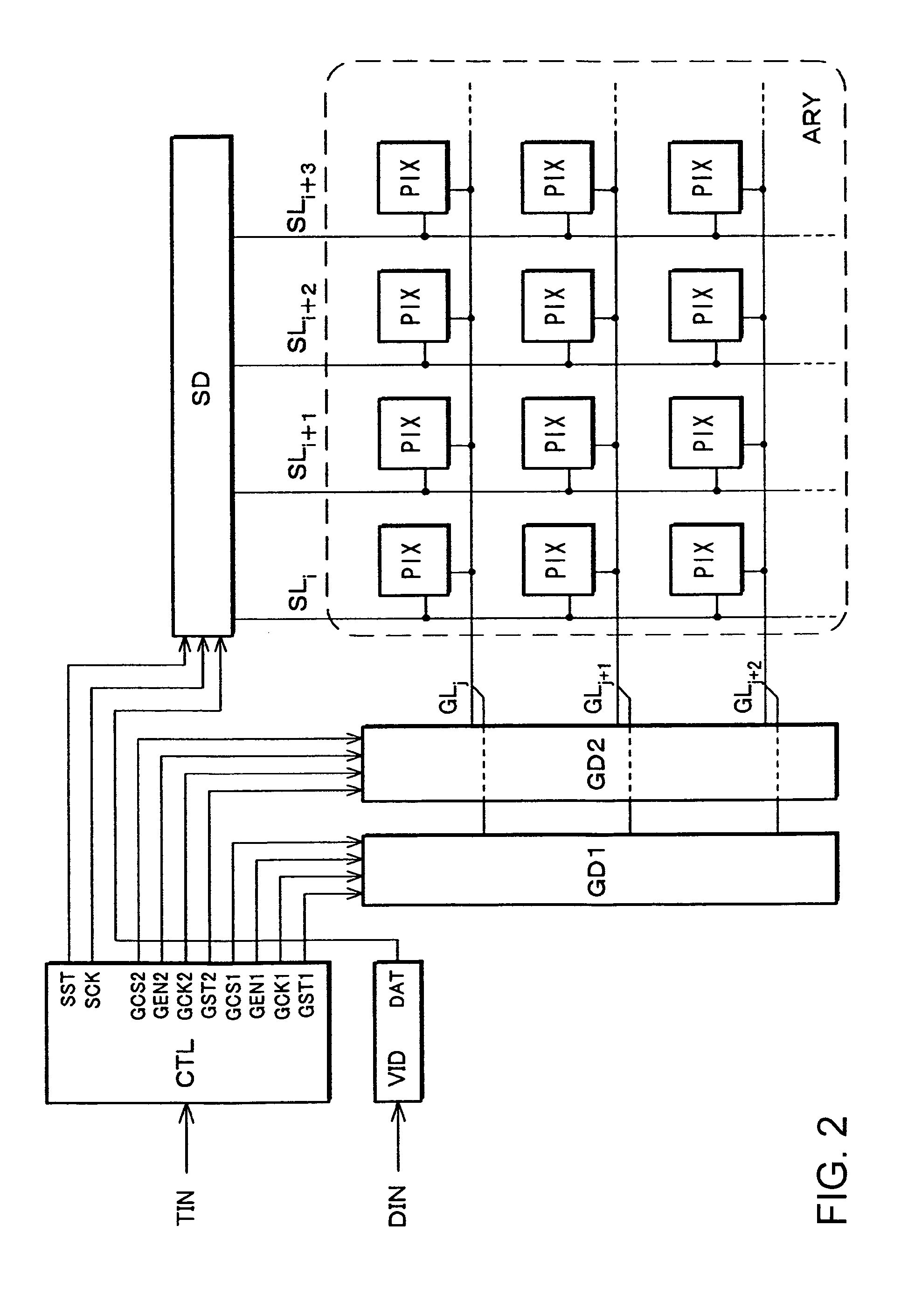
[Embodiment 2]
[0490]Referring to FIG. 93 to FIG. 96, the following will describe another embodiment in accordance with the present invention.
[0491]FIG. 93 is a block diagram showing, as an example, a configuration of an image display device of the present embodiment. The present image display device is composed of a multitone analog data signal line drive circuit ANSD and scan signal line drive circuit GD, a binary data signal line drive circuit BINSD, data signal lines SLn (1≦n≦i), scan signal lines GLn (1≦n≦j), pixels PIX, a control signal circuit CTRL, a binary data storage section BINMEM, and a multitone data storage section DATMEM.
[0492]The analog data signal line drive circuit ANSD includes a shift register SR1 and sampling section SAMP which operate in synchronism with a clock signal CK. The multitone analog data signal line drive circuit ANSD may be replaced with a drive circuit for binary analog data, drive circuit for digital data, or a drive circuit for a binary digital d...
embodiment 3
[Embodiment 3]
[0504]Referring to FIG. 97, the following will describe still another embodiment in accordance with the present invention. Here, for convenience, members of the present embodiment that have the same arrangement and function as members shown in a figure of any one of the previous embodiments, and that are mentioned in that embodiment are indicated by the same reference numerals and description thereof is omitted.
[0505]In the present embodiment, a display state switching signal PICST is separately inputted to the output control section CNTTRF constituting the binary data signal line drive circuit BINSD. FIG. 97 is a block diagram showing the binary data signal line drive circuit BINSD in such a case. In embodiment 2, either the for-turn-on potential VW or the for-non-turn-on potential VB is supplied to the data signal line only when the binary data signal DIGDAT is meaningful. In contrast, in the present embodiment, the output control section CNTTRF operates as follows: ...
PUM
| Property | Measurement | Unit |
|---|---|---|
| temperature | aaaaa | aaaaa |
| temperatures | aaaaa | aaaaa |
| drive voltage | aaaaa | aaaaa |
Abstract
Description
Claims
Application Information