System and method for determining a carrier layout using cornered chip-to-chip input/output

a chip-to-chip input/output and carrier layout technology, applied in the field of integrated circuit carrier layout, can solve the problems of non-attainable neighbor problem, accesses can also potentially create contentioned pathways, etc., and achieve the effect of reducing hamming distan

Active Publication Date: 2007-03-13
ORACLE INT CORP
View PDF4 Cites 22 Cited by
  • Summary
  • Abstract
  • Description
  • Claims
  • Application Information

AI Technical Summary

Benefits of technology

[0009]One embodiment provides a system and method for determining a carrier layout using cornered chip-to-chip input / output. Each of a plurality of individual integrated circuit carriers communicatively interfaceable through cornered input / output ports is oriented at a uniform rotation relative to an edge of a carrier layout. Each carrier defines a set of rectilinear edges. Each carrier is placed juxtaposed at an open corner to at least one other carrier within a rectilinear lattice topologically arranged in the carrier layout to substantially minimize Hamming distances between each of the carriers.

Problems solved by technology

In addition, the corner carriers 11, in particular, provide only a single cornered I / O interface 15, which violates the two routes between each peer property and creates a non-attainable neighbor problem.
However, cross-carrier layout memory accesses can also potentially create contentioned pathways in the external networks of those diamond carrier layouts being crossed.

Method used


Image

  • System and method for determining a carrier layout using cornered chip-to-chip input/output
  • System and method for determining a carrier layout using cornered chip-to-chip input/output
  • System and method for determining a carrier layout using cornered chip-to-chip input/output

Examples


Embodiment Construction

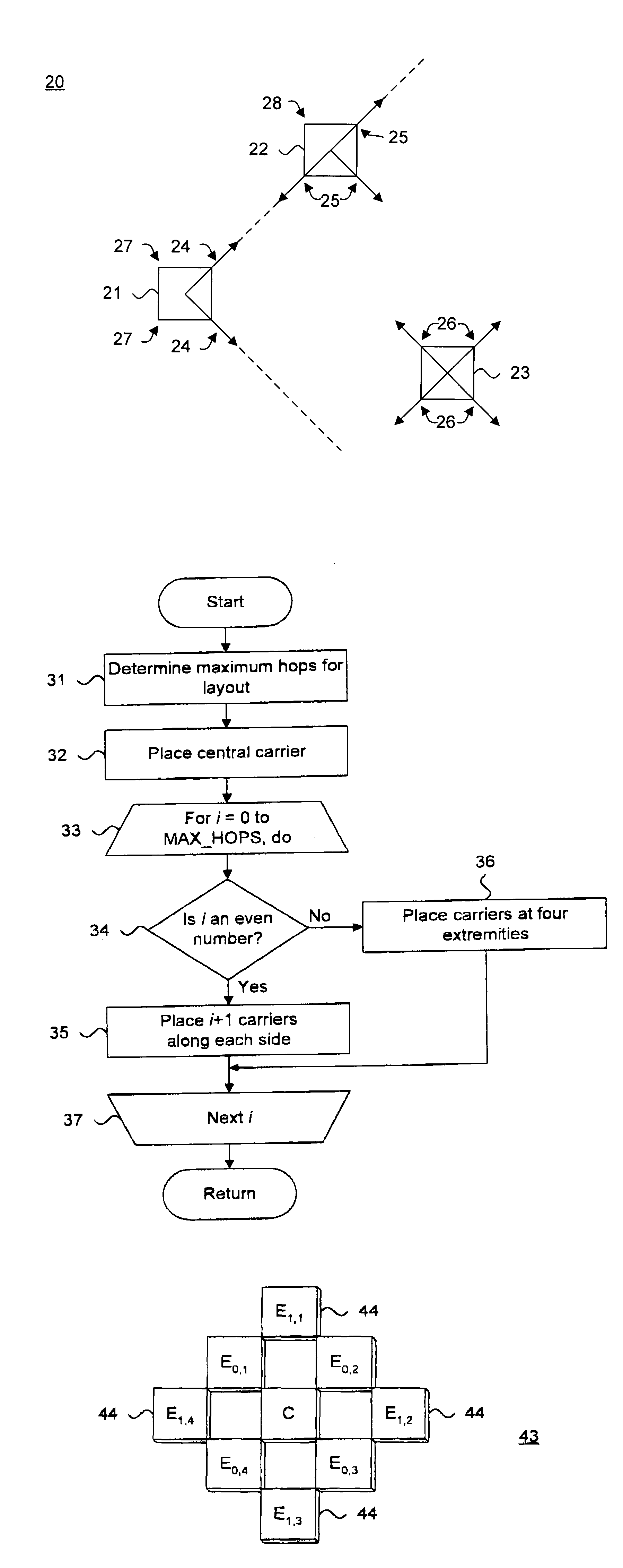
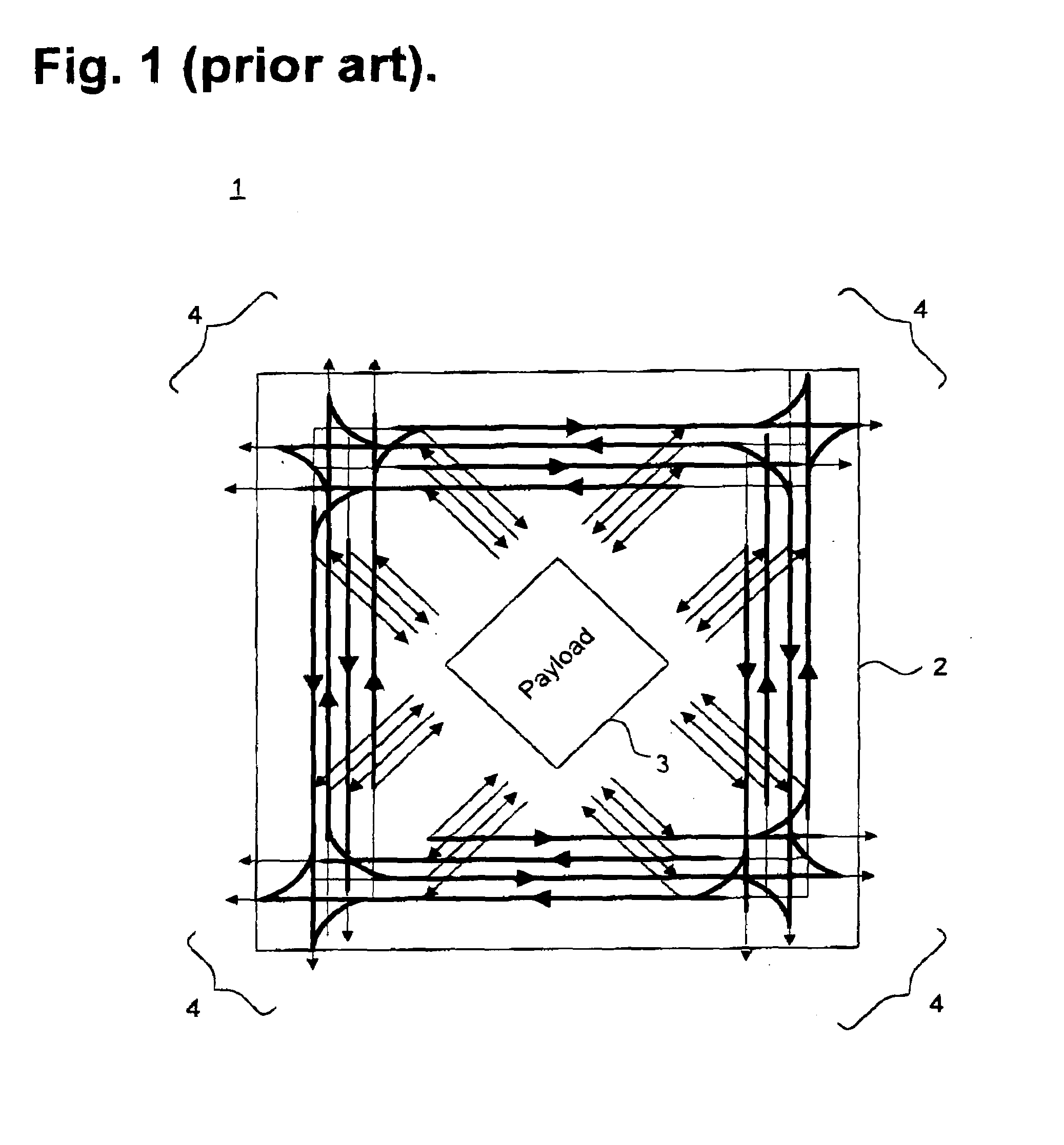
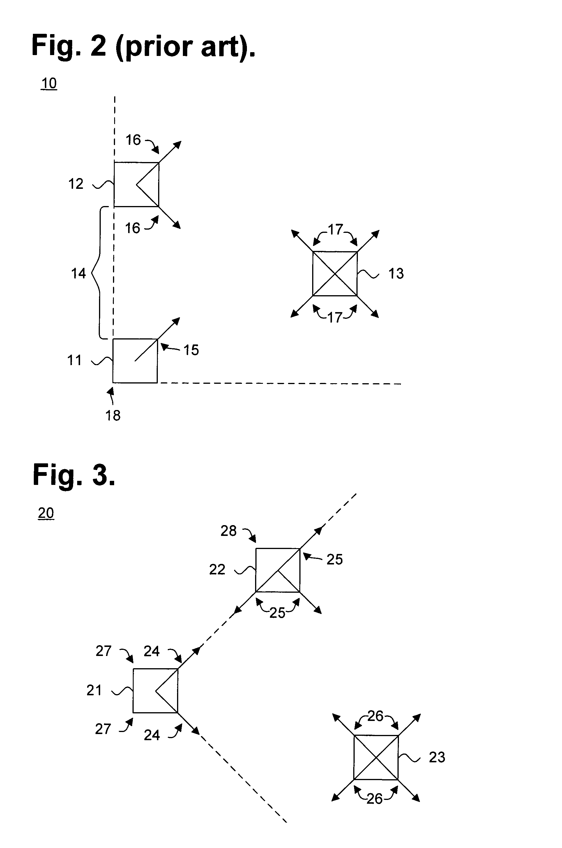
[0023]FIG. 1 is a functional block diagram showing a prior art chip 1 using cornered I / O. The chip 1 includes a carrier 2 and a functionally-defined integrated circuit payload 3. The payload 3 can include a processor, memory or I / O device, and is interfaced to other carriers by a set of cornered I / O interfaces 4 to provide chip-to-chip interconnections.

[0024]In the described embodiment, chips 1 overlap at the corners and a pair of two-dimensional grids are formed within each chip 1. The first grid forms a main network that includes the carrier side wires and switches and the second grid forms an access network connecting the payload 3 to carrier wires and switches, also referred to as I / O ports. Thus, the set of main networks formed by interconnected chips 1 logically define a crossbar switching network with access networks appearing within the crosses rotated at a 45-degree angle.

[0025]Communication between individual chips 1 is provided by packet routing. In the described embodime...


PUM


Abstract

A system and method for determining a carrier layout using cornered chip-to-chip input/output is presented. Each of a plurality of individual integrated circuit carriers communicatively interfaceable through cornered input/output ports is oriented at a uniform rotation relative to an edge of a carrier layout. Each carrier defines a set of rectilinear edges. Each carrier is placed juxtaposed at an open corner to at least one other carrier within a rectilinear lattice topologically arranged in the carrier layout to substantially minimize Hamming distances between each of the carriers.

Description

GOVERNMENT LICENSE RIGHTS[0001]This invention was made with United States Government support under Contract No. NBCH020055 awarded by the Defense Advanced Research Projects Administration. The United States Government has certain rights in the invention.FIELD OF THE INVENTION[0002]The invention relates in general to integrated circuit carrier layout and, in particular, to a system and method for determining a carrier layout using cornered chip-to-chip input / output.BACKGROUND OF THE INVENTION[0003]Conventionally, circuit carriers provide physical housings for integrated circuits and include a set of pins provided along the side or bottom of each carrier for interfacing the integrated circuit to an external environment. Each integrated circuit performs a specific function, such as processing or storage, and the integrated circuit and carrier combinations are generally generically termed chips. The individual carrier pins typically interconnect to a circuit board bus defining a shared ...

Claims


Application Information

Patent Timeline
Patent Type & Authority Patents(United States)
IPC IPC(8): G06F17/50
CPCH04L45/122H04L45/06
Inventor TOURANCHEAU, BERNARDVIGOUROUX, XAVIER-FRANCOISKOCH-HOFER, CEDRIC
Owner ORACLE INT CORP
Why Eureka
Try Eureka