Multi-layered printed wiring board

a printed wiring board and multi-layer technology, applied in the direction of printed circuit aspects, cross-talk/noise/interference reduction, circuit electrical arrangement, etc., can solve the problems of increasing the time and cost required for manufacturing printed wiring boards, and the difficulty of high-density wiring, so as to reduce radiation noise

Inactive Publication Date: 2007-04-03
CANON KK
View PDF12 Cites 2 Cited by
  • Summary
  • Abstract
  • Description
  • Claims
  • Application Information

AI Technical Summary

Benefits of technology

[0011]It is therefore an object of the present invention to provide a multi-layered printed wiring board that is capable of securing required wiring density even with a decreased number of wiring layers and reducing radiation noises.

Problems solved by technology

The increase in the number of layers as in the first prior art to accommodate all required lines easily realizes high-density wiring, but increases the time and cost required for manufacturing the printed wiring board.
Providing ground lines and power supply lines in the form of a grid on each of the wiring layers as in the second prior art reduces radiation noises, but imposes a lot of restrictions on a space for wiring signal lines and makes it difficult to achieve high-density wiring.

Method used


Image

  • Multi-layered printed wiring board
  • Multi-layered printed wiring board
  • Multi-layered printed wiring board

Examples


first embodiment

(First Embodiment)

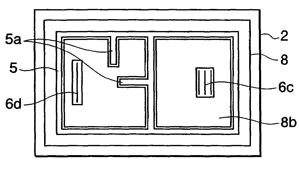
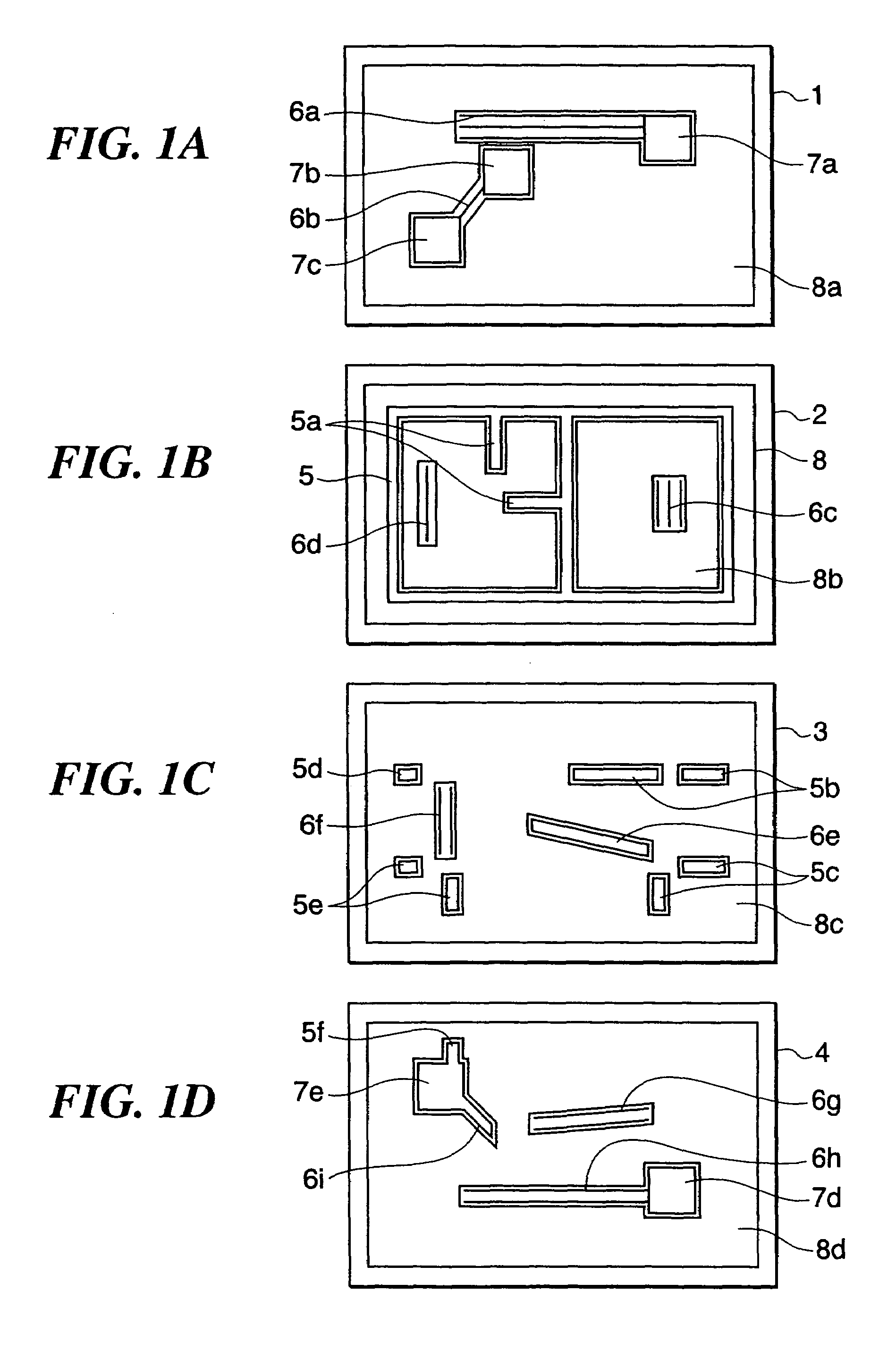
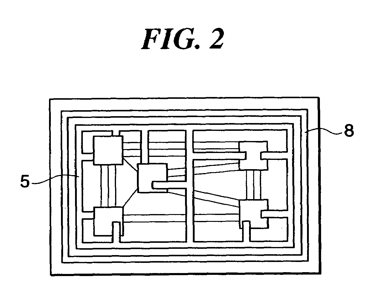
[0046]FIGS. 1A–1D are schematic diagrams showing the construction of a multi-layered printed wiring board according to a first embodiment of the present invention. FIG. 2 is a schematic diagram showing the construction of all layers of the multi-layered printed wiring board according to the first embodiment as viewed from above, and is intended to provide a supplemental explanation of the connection and positional relationship between signal lines.

[0047]The multi-layered printed wiring board according to the first embodiment is comprised of a first wiring layer 1, a second wiring layer 2, a third wiring layer 3, and a fourth wiring layer 4, which are shown in FIGS. 1A–1D, respectively. These wiring layers are laminated one upon another in the order mentioned. Each of the wiring layers are comprised of a substrate, and various wiring lines provided on a surface of the substrate. This basic construction applies to other embodiments, described later.

[0048]As shown in ...

second embodiment

(Second Embodiment)

[0066]FIGS. 5A–5D are schematic diagrams showing the construction of a multi-layered printed wiring board according to a second embodiment of the present invention.

[0067]The multi-layered printed wiring board according to the second embodiment supplies power to electronic parts 17a, 17b, 17c driven at a first voltage, and electronic parts 17a′, 17b′ driven at a second voltage different from the first voltage.

[0068]The multi-layered printed wiring board according to the second embodiment is comprised of a first wiring layer 11, a second wiring layer 12, a third wiring layer 13, and a fourth wiring layer 14. The electronic parts driven at different two voltages are mounted on the first wiring layer 11 and the fourth wiring layer 14.

[0069]As shown in FIG. 5A, the electronic parts 17a, 17b, 17c driven at the first voltage and the electronic parts 17a′, 17b′ driven at the second voltage are mounted on the first wiring layer 11, and signal lines 16a, 16b and a ground pa...

third embodiment

(Third Embodiment)

[0077]FIGS. 6A–6D are schematic diagrams showing the construction of a multi-layered printed wiring board according to a third embodiment of the present invention. FIG. 7 is a schematic diagram showing the construction of all layers of the multi-layered printed wiring board according to the third embodiment when they are fluoroscopically viewed from above, and is intended to provide a supplemental description of the connection and positional relationship between signal lines.

[0078]The multi-layered printed wiring board according to the third embodiment supplies power to electronic parts 27a, 27b, 27c driven at a first voltage, and electronic parts 27a′, 27b′ driven at a second voltage different from the first voltage.

[0079]The multi-layered printed wiring board according to the second embodiment is comprised of a first wiring layer 21, a second wiring layer 22, a third wiring layer 23, and a fourth wiring layer 24. The electronic parts driven at two different volta...


PUM


Abstract

A multi-layered printed wiring board, capable of securing required wiring density even with a decreased number of wiring layers and reducing radiation noises, has at least three wiring layers each at least having at least one power supply line or a ground line, and another kind of line, the wiring layers each having an outer edge. A ground line is formed at the outer edge of at least one of the wiring layers. A basic power supply line is formed inside the ground line. At least one power supply line extends from the basic power supply line. A plurality of electronic parts are mounted on at least one of the wiring layers. The at least one power supply line is wired to mounting positions of the electronic parts via at least one of the wiring layers.

Description

[0001]This application is a division of application Ser. No. 10 / 046,163, filed Jan. 16, 2002 now U.S. Pat. No. 6,800,814.BACKGROUND OF THE INVENTION[0002]1. Field of the Invention[0003]This invention relates to a multi-layered printed wiring board having a plurality of wiring layers, and more particularly to a multi-layered printed wiring board that is suitably applied to achieve high-density wiring.[0004]2. Description of the Related Art[0005]In recent years, with the advancement of functions of digital equipment, an increasing number of printed wiring boards installed on digital equipment have been equipped with a great number of multi-pin packaged semiconductor devices such as the BGA (Ball Grid Array). Such multi-pin packaged semiconductor devices include integrated circuits having 500 pins or more. The wiring density of such printed wiring boards has been raised with the increase in the number of pins. This necessitates increasing the number of wiring layers of printed wiring b...

Claims


Application Information

Patent Timeline
Patent Type & Authority Patents(United States)
IPC IPC(8): H01R12/04H05K1/11H05K1/02H05K3/46
CPCH05K1/0216H05K2201/09336H05K2201/09345H05K2201/09354
Inventor OHSAKA, TOHRU
Owner CANON KK
Why Eureka
Try Eureka