Printed circuit board

a printed circuit board and circuit board technology, applied in the direction of printed circuit aspects, non-printed electrical components of printed circuits, cross-talk/noise/interference reduction, etc., can solve the problems of radiation noise, noise increase, deviation in the operation timing of the reception-side semiconductor package, etc., to achieve high-density wiring and reduce radiation noise

Active Publication Date: 2013-10-24
CANON KK
View PDF7 Cites 10 Cited by
  • Summary
  • Abstract
  • Description
  • Claims
  • Application Information

AI Technical Summary

Benefits of technology

[0010]The present invention provides a printed circuit board with which radiation noise is reduced and a high density wiring is realized by securing a return current path with respect to a signal current.
[0012]According to the aspect of the present invention, the high density wiring and the high density mounting of the printed circuit board can be realized while the radiation noise is reduced by securing the return path for the signal current.

Problems solved by technology

If a large difference exists in the lengths of the respective wirings, an operational timing of the reception-side semiconductor package is deviated, and noise is increased because of a difference in the timing at which the signals are reflected at connection points of the respective wirings.
Thus, radiation noise is increased.
It is therefore difficult to arrange the bus wirings at equal distances.
When the number of bus wirings is increased in the case of the multi-layered printed wiring board, the number of the via holes prepared in the ground layer or the power supply layer of the signal wirings is increased, and it is difficult to secure the return path for the signal.
As described in Japanese Patent Laid-Open No. 8-340161, even when the via holes are prepared in a diagonal manner, the area for preparing the via holes is enlarged, and a degree of freedom for the board design is largely impaired.
That is, if the via holes are prepared in a diagonal manner, the area for mounting electronic components such as bypass capacitors is limited, and the area for forming the other signal wirings is also limited.

Method used


Image

  • Printed circuit board
  • Printed circuit board
  • Printed circuit board

Examples


first exemplary embodiment

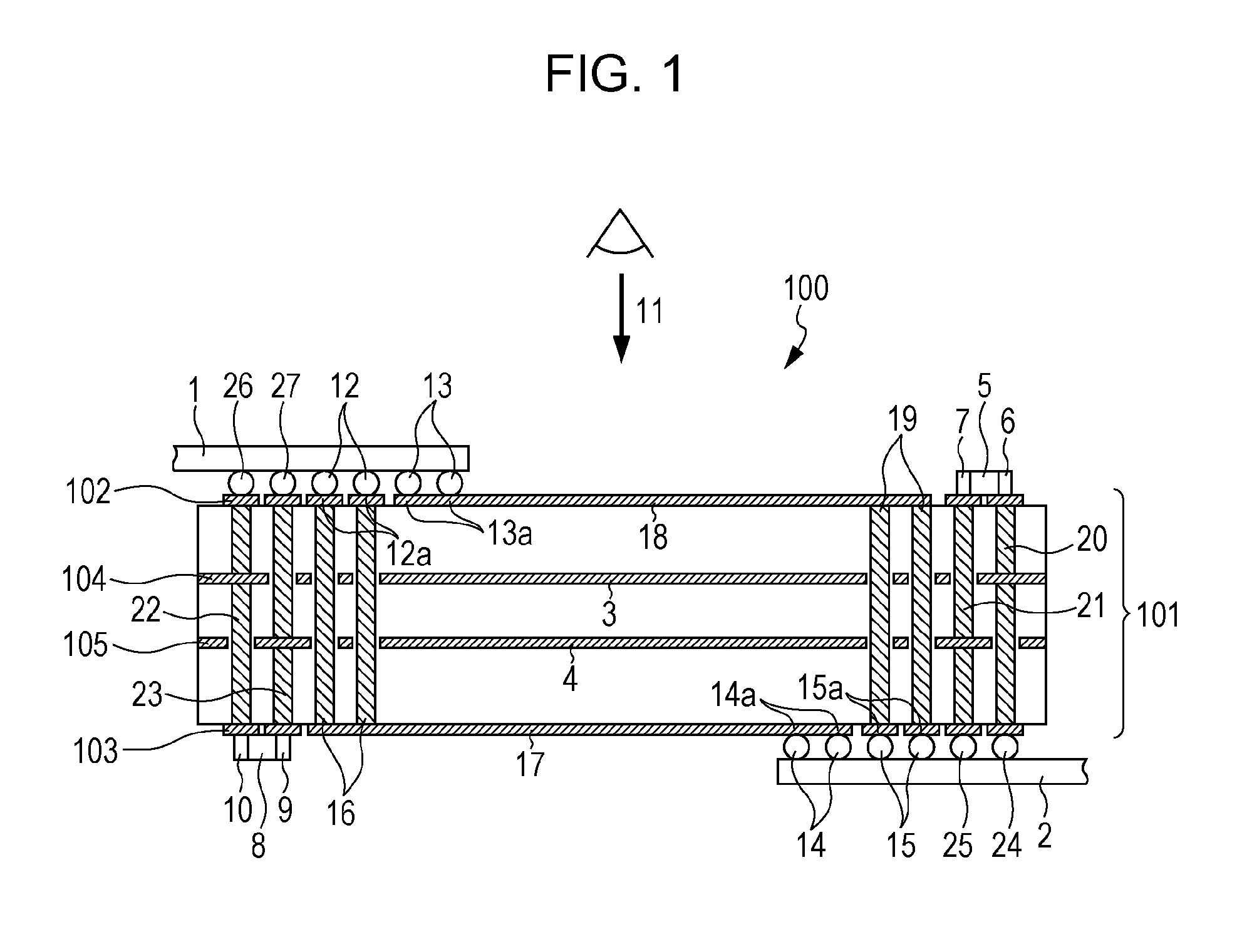
[0020]FIG. 1 is a cross sectional view of a multi-layered printed circuit board 100 having a four-layer structure according to a first exemplary embodiment of the present invention. In the multi-layered printed circuit board 100, a first semiconductor package 1 on a transmission side is mounted on a first signal layer 102 corresponding to a first layer (first surface layer) of a printed wiring board 101, and a second semiconductor package 2 on a reception side is mounted on a second signal layer 103 corresponding to a fourth layer (second surface layer). The second layer provided between the first layer and the fourth layer is a ground layer 104, and the third layer is a power supply layer 105. A ground pattern 3 is formed on the ground layer 104, and a power supply pattern 4 is formed on the power supply layer 105. The second layer may be set as the power supply layer 105, and the third layer may be set as the ground layer 104. The same applies when the second semiconductor package...

second exemplary embodiment

[0037]FIG. 4 is a cross sectional view of a printed circuit board having a four-layer structure according to a second exemplary embodiment of the present invention. To simplify the description, only a part of semiconductor packages 28 and 29 which will be described below is illustrated.

[0038]FIG. 4 is a cross sectional view of a multi-layered printed circuit board 200 having a four-layer structure according to the second exemplary embodiment of the present invention. In the multi-layered printed circuit board 200, a first semiconductor package 28 on a transmission side is mounted on a power supply layer 205 corresponding to the first layer (first surface layer) of the printed wiring board 201, and a second semiconductor package 29 on a reception side is mounted on the ground layer 204 corresponding to the fourth layer (second surface layer). A power supply pattern 30 is formed on the power supply layer 205, and a ground pattern 31 is formed on the ground layer 204. The second layer ...

third exemplary embodiment

[0044]The printed circuit board having the four-layer structure has been described according to the first and second exemplary embodiments. However, the embodiment of the present invention is not limited to the above and can be applied to a multi-layered printed circuit board having four or more layers. FIG. 5 illustrates a case of a printed circuit board having a six-layer structure.

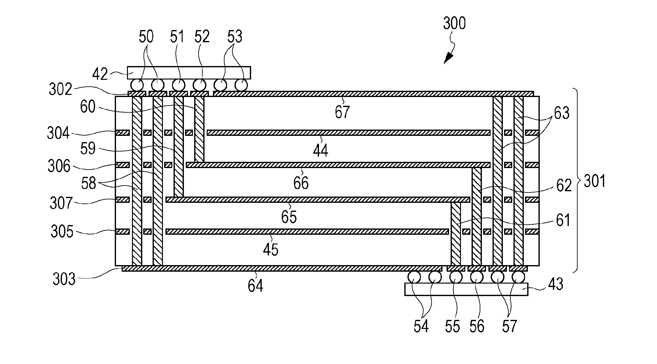
[0045]FIG. 5 is a cross sectional view of a multi-layered printed circuit board 300 having a six-layer structure according to a third exemplary embodiment of the present invention. In the multi-layered printed circuit board 300, a first semiconductor package 42 on a transmission side is mounted on a first signal layer 302 corresponding to the first layer (first surface layer) of a printed wiring board 301, and a second semiconductor package 43 on a reception side is mounted on a second signal layer 303 corresponding to a sixth layer (second surface layer). The second layer arranged on an inner layer bet...


PUM


Abstract

A printed circuit board includes a first semiconductor package on a first surface layer of a printed wiring board and a second semiconductor package on a second surface layer where a bus signal is transmitted from the first to the second semiconductor package. A first bus wiring path from a signal terminal on an inner circumference side of the first semiconductor package via a via hole and the second surface layer to a signal terminal on an outer circumference side of the second semiconductor package and a second bus wiring path from a signal terminal on an outer circumference side of the first semiconductor package via the second surface layer and a via hole to a signal terminal on an inner circumference side of the second semiconductor package are provided, thus securing a return current path for a signal current and realizing a high density wiring while suppressing radiation noise.

Description

BACKGROUND OF THE INVENTION[0001]1. Field of the Invention[0002]The present invention relates to a bus wiring formed on a printed circuit board.[0003]2. Description of the Related Art[0004]A higher speed in operations and a higher density of wirings are demanded for a printed circuit board along with sophistication of electronics devices in recent years. For that reason, a bus wiring is frequently used in which plural signal lines through which a signal can be transmitted at a high speed are arranged in parallel. In a case where the signals are transmitted by using the bus wiring from a transmission-side semiconductor package to a reception-side semiconductor package, lengths of respective wirings are set to be equal to each other. If a large difference exists in the lengths of the respective wirings, an operational timing of the reception-side semiconductor package is deviated, and noise is increased because of a difference in the timing at which the signals are reflected at connec...

Claims


Application Information

Patent Timeline
Patent Type & Authority Applications(United States)
IPC IPC(8): H05K1/18
CPCH05K1/181H05K1/0228H05K1/0231H05K1/0243H05K2201/10545H05K2201/10734H01L2224/16225H01L2924/15174H05K1/025H05K1/0298H01L25/0657H01L2225/06548H01L2225/06555H05K1/115H05K2201/09654
Inventor ISONO, HIROSHI
Owner CANON KK
Why Eureka
Try Eureka