Photovoltaic cell and method of fabricating the same

a photovoltaic cell and photovoltaic technology, applied in the field of photovoltaic cells, can solve the problems of reducing the number of photons incident on the n-type single-crystalline silicon substrate, recombination of carriers to lower the open-circuit voltage voc, and limited power generation efficiency

Active Publication Date: 2007-04-03
SANYO ELECTRIC CO LTD
View PDF9 Cites 56 Cited by
  • Summary
  • Abstract
  • Description
  • Claims
  • Application Information

AI Technical Summary

Benefits of technology

[0010]It is an object of the present invention to provide a photovoltaic cell and a method of fabricating the same which allows for the maximum use of incident light.
[0011]It is another object of the present invention to provide a photovoltaic cell and a method of fabricating the same which allows for the maximum use of incident light with reduced manufacturing cost and manufacturing time.

Problems solved by technology

At the junction of the n-type single-crystalline substrate and the p-type amorphous silicon film, however, there are multiple interface states, causing recombination of carriers to lower the open-circuit voltage Voc.
In the above photovoltaic cell, however, the electrode and the p-type amorphous silicon film on the main-surface side absorbs light, causing the number of photons incident on the n-type single-crystalline silicon substrate to be decreased, resulting in limited power generation efficiency.
In addition, the above photovoltaic cell comprises a large number of layers, causing its manufacturing processes to be complex and manufacturing cost expensive.

Method used


Image

  • Photovoltaic cell and method of fabricating the same
  • Photovoltaic cell and method of fabricating the same
  • Photovoltaic cell and method of fabricating the same

Examples


##ventive example 1

Inventive Example 1

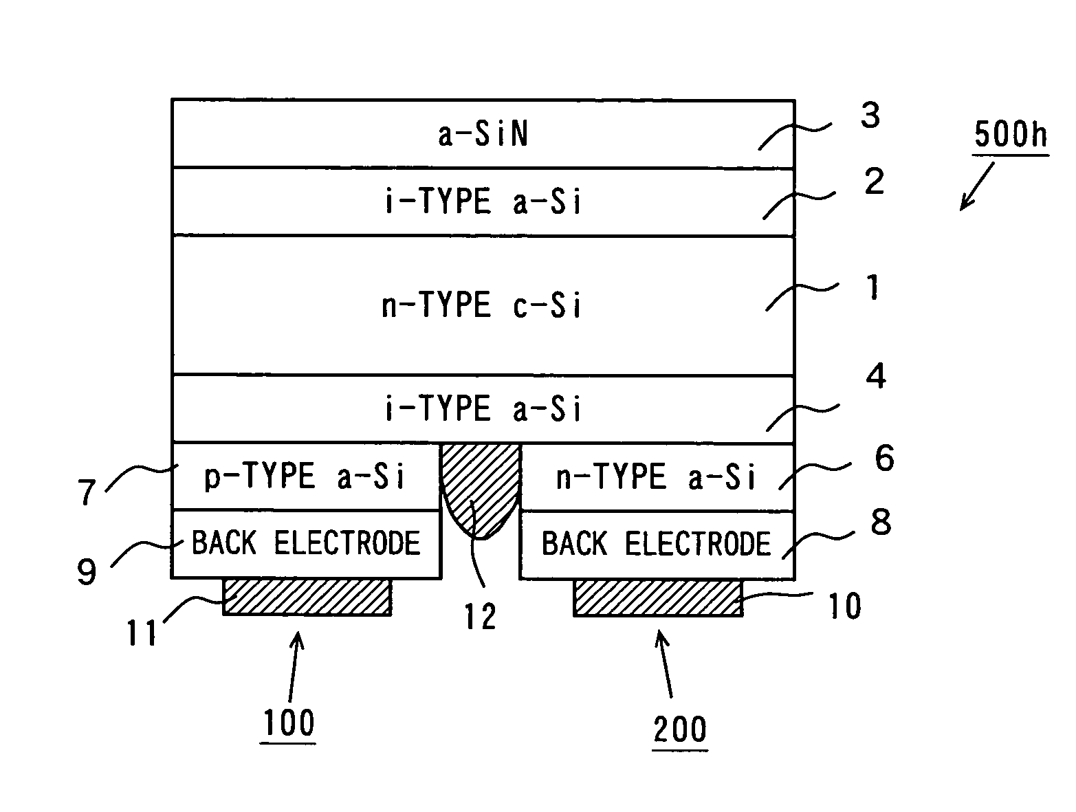
[0187]In the Example below, a photovoltaic cell 500c having the structure of FIG. 5 was fabricated in the method of the above-described embodiment, for measurement of output characteristics. Table 2 shows conditions under which the photovoltaic cell of the Inventive Example was fabricated.

[0188]

TABLE 2FORMATION CONDITIONSRFSUBSTRATEPOWERFILMTEMPERATUREUSED GASPRESSUREDENSITYTHICKNESSTREATMENT(° C.)(sccm)(Pa)(mW / cm2)(nm)p-i-TYPE170H2: 0~1000408.3315SIDEAMORPHOUSSiH4: 40SILICONFILMp-TYPE170H2: 0~1000408.3310AMORPHOUSSiH4: 40SILICONB2H6 (2%): 40FILMn-i-TYPE170H2: 0~1000408.3315SIDEAMORPHOUSSiH4: 40SILICONFILMn-TYPE170H2: 0~1000408.3315AMORPHOUSSiH4: 40SILICONPH3 (1%): 40FILM

[0189]As shown in Table 2, in the formation of a p-type amorphous silicon film 7, B2H6 gas diluted with H2 gas was used with the concentration of B2H6 being set to 2% for SiH4. In the formation of an n-type amorphous silicon film 6, on the other hand, PH3 gas diluted with H2 gas was used with the ...


PUM

PropertyMeasurementUnit
thicknessaaaaaaaaaa
thicknessaaaaaaaaaa
thicknessaaaaaaaaaa

Abstract

An i-type amorphous silicon film and an anti-reflection film made of amorphous silicon nitride or the like are formed in this order on a main surface of an n-type single-crystalline silicon substrate. On a back surface of the n-type single-crystalline silicon substrate are provided a positive electrode and a negative electrode next to each other. The positive electrode includes an i-type amorphous silicon film, a p-type amorphous silicon film, a back electrode, and a collector electrode formed in this order on the back surface of the n-type single-crystalline silicon substrate. The negative electrode includes an i-type amorphous silicon film, an n-type amorphous silicon film, a back electrode, and a collector electrode formed in this order on the back surface of the n-type single-crystalline silicon substrate.

Description

BACKGROUND OF THE INVENTION[0001]1. Field of the Invention[0002]The present invention relates to a photovoltaic cell using a semiconductor junction and a method of fabricating the same.[0003]2. Description of the Background Art[0004]In recent years, a photovoltaic cell having a junction of an n-type single-crystalline silicon substrate and a p-type amorphous silicon film has been developed. In order to enhance photoelectric conversion efficiency of such a photovoltaic cell, it is necessary to enhance fill factor F.F. while maintaining high short-circuit current Isc and open-circuit voltage Voc.[0005]At the junction of the n-type single-crystalline substrate and the p-type amorphous silicon film, however, there are multiple interface states, causing recombination of carriers to lower the open-circuit voltage Voc.[0006]For this reason, in order to suppress such recombination of carriers at the junction of an n-type single-crystalline silicon substrate and a p-type amorphous silicon fi...

Claims


Application Information

Patent Timeline
Patent Type & Authority Patents(United States)
IPC IPC(8): H01L29/04H01L31/036H01L31/0376H01L31/20H01L31/075
CPCH01L31/0747H01L31/075Y02E10/548H01L31/022441Y02E10/50
Inventor TERAKAWA, AKIRAASAUMI, TOSHIO
Owner SANYO ELECTRIC CO LTD
Why Eureka
Try Eureka