High speed voltage level translator

a translator and high-speed technology, applied in the direction of pulse automatic control, logic circuit, pulse technique, etc., can solve the problems of increasing difficulty, device is very slow, and glitches due to bootstrapping, so as to reduce the integrated circuit area, eliminate glitches, and minimize power dissipation

Active Publication Date: 2007-04-03
STMICROELECTRONICS PVT LTD
View PDF11 Cites 10 Cited by
  • Summary
  • Abstract
  • Description
  • Claims
  • Application Information

AI Technical Summary

Benefits of technology

[0006]According to an embodiment of the present invention, a high speed voltage level translator circuit is provided having a reduced integrated circuit area. The translator circuit according to an embodiment of the present invention can be used for translating a low voltage level to a high voltage level with minimized power dissipation by using a feedback arrangement that substantially eliminates glitches. The translator circuit of the present invention can be built with sub 0.1 micron technology.

Problems solved by technology

MOS devices compatible with higher voltages are required to be driven by lower voltages, which is increasingly difficult as the technology of the core moves towards lower dimension regimes.
When the gate of these transistors is driven by signals having a lower voltage swing, the device is very slow, needing a large area to drive the output at the desired slew rate.
Another problem with the circuit shown in FIG. 1 is that whenever the OUT signal at node 14 is rising, there is a glitch due to bootstrapping.

Method used


Image

  • High speed voltage level translator
  • High speed voltage level translator
  • High speed voltage level translator

Examples


Embodiment Construction

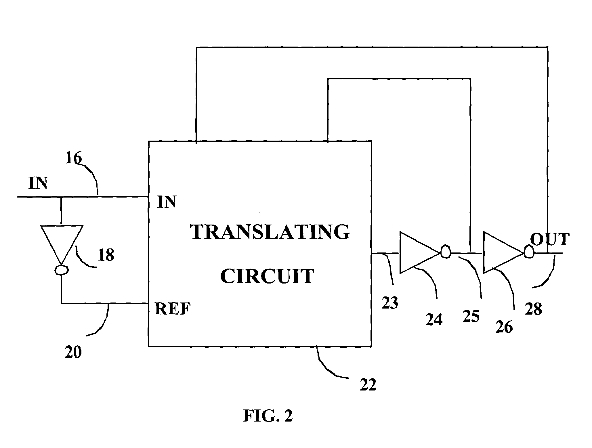
[0015]FIG. 2 shows a block diagram of the translator circuit according to the present invention. Translating circuit 22 includes an input terminal, an output terminal, and two feedback terminals, as well as power and ground terminals, which are not shown in FIG. 2. Input to translating circuit 22 is provided by the core input signal IN at node 16. The output of the translating circuit 22 at node 23 is driven by a pair of inverters 24 and 26 to get a full voltage swing at the output node 28. Feedback signals at nodes 25 and 28 are fed back to the translating circuit 22 to minimize power dissipation.

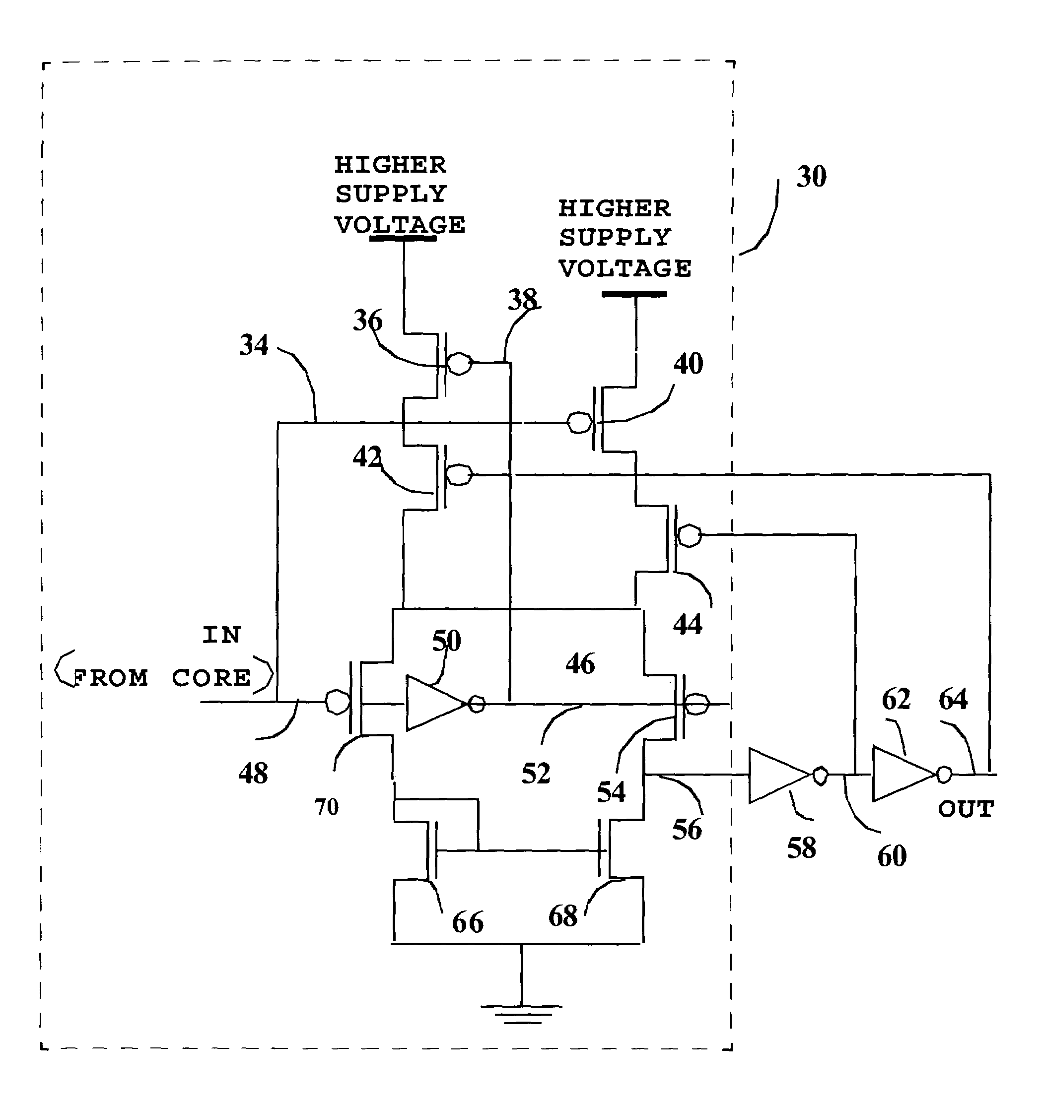
[0016]FIG. 3 is a schematic diagram of the present invention for a transistor-level embodiment. Translating circuit 30 is used for translating a low voltage swing to a high voltage swing. Translating circuit 30 according to an embodiment of the present invention is biased by four different P-channel transistors 36, 40, 42 and 44. These transistors provide biasing current to the translating...


PUM


Abstract

A high speed voltage level translator having minimum power dissipation and reduced area, specifically in the sub 0.1 micron domain, includes a transistorized arrangement to receive a low voltage input signal and to control current in the translated high level voltage signal. The translator further provides a differential amplifier arrangement for receiving the low level voltage input signal and provides feedback signals to the transistorized arrangement thereby outputting a high level voltage translated signal.

Description

FIELD OF THE INVENTION[0001]This invention relates to high speed translation of low core voltage to I / O voltage. In particular it relates to an improved voltage level translation in devices with reduced size as in sub 0.1-micron technology having minimum power dissipation and less area.BACKGROUND OF THE INVENTION[0002]As technology has progressed, the size of integrated circuit devices has minimized to very deep sub-micron technology and further towards sub-0.1 micron technology, consequently reducing the operating voltage of the device core. However, I / O circuits keep operating at higher voltages than the core as they must interface with other devices operating at higher voltage.[0003]MOS devices compatible with higher voltages are required to be driven by lower voltages, which is increasingly difficult as the technology of the core moves towards lower dimension regimes.[0004]To achieve core voltage to I / O translation, conventional translators uses latch type circuit. FIG. 1 illust...

Claims


Application Information

Patent Timeline
Patent Type & Authority Patents(United States)
IPC IPC(8): H03L5/00H03K19/0185
CPCH03K19/018528
Inventor DUBEY, HARI BILASHVIJ, ANSHU
Owner STMICROELECTRONICS PVT LTD
Why Eureka
Try Eureka