Optically enabled hybrid semiconductor package

a hybrid semiconductor and integrated technology, applied in the field of printed circuit boards, can solve the problems of difficult and time-consuming steps, and achieve the effects of high yield, high volume finished parts, and quick and easy integration

Active Publication Date: 2007-04-03
REFLEX PHOTONICS
View PDF19 Cites 11 Cited by
  • Summary
  • Abstract
  • Description
  • Claims
  • Application Information

AI Technical Summary

Benefits of technology

[0008]This invention provides concepts that are directed towards the manufacturability of volume quantities of OE-PCBs. With these concepts, components and sub-components can be quickly and easily integrated with printed wiring boards and optical waveguides in a reliable manner to achieve high-yield, high volume finished parts.

Problems solved by technology

One of the major difficulties faced in the integration of optoelectronic packages with printed wiring boards (PWB), is to couple efficiently the light between optoelectronic devices and optical waveguides provided on a PWB.
However, this alignment step is difficult to achieve and is thus time-consuming.
However this method still comprises the step of aligning the rod with respect to the VCSEL and with respect to the embedded waveguide, which can be difficult and time consuming.

Method used


Image

  • Optically enabled hybrid semiconductor package
  • Optically enabled hybrid semiconductor package
  • Optically enabled hybrid semiconductor package

Examples


Embodiment Construction

[0026]In the following description of the embodiments, reference to the accompanying drawings are by way of illustration of an example by which the invention may be practiced. It will be understood that other embodiments may be made without departing from the scope of the invention disclosed.

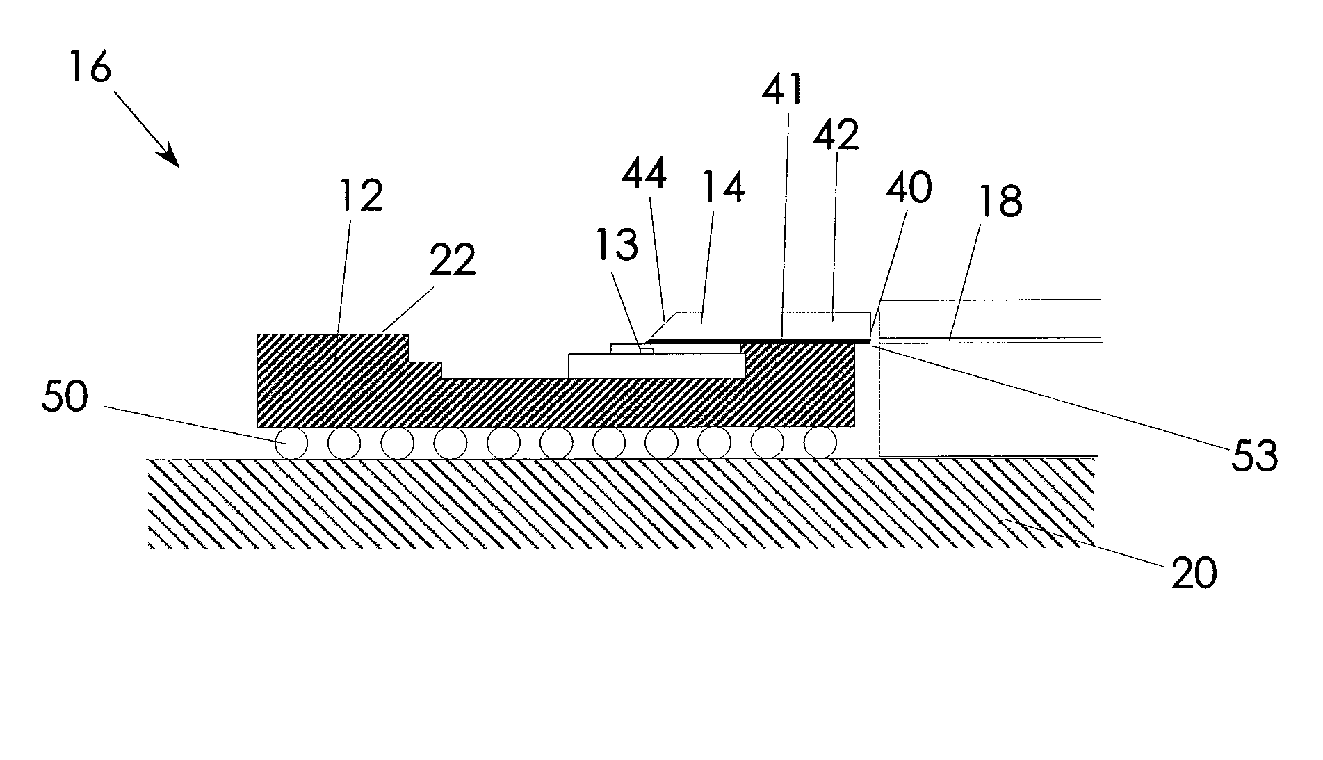
[0027]In one embodiment of the present invention, an integrated circuit (IC) package is modified to accept an optical sub assembly (OSA) in order to form an optical hybrid IC (OHIC) package, which can then be easily side-coupled to an optical waveguide of a printed circuit board (PWB) to form an optically enabled printed circuit board (OE-PCB).

Integrated Circuit (IC) Packages

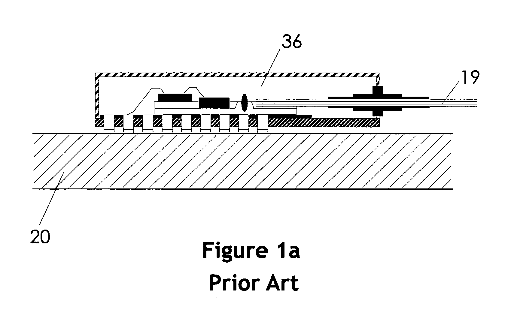
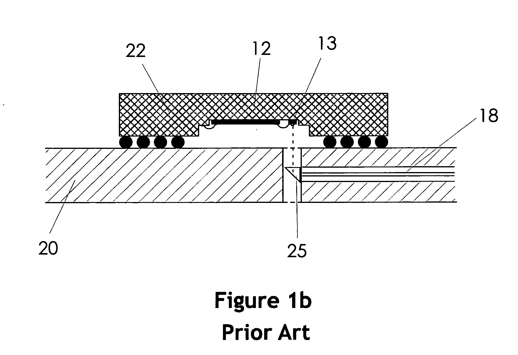
[0028]Integrated circuit (IC) packages 12 are standard mechanical / electrical housings to semiconductor chips. They are used to electrically connect the fragile semiconductor chip's electrical signals to a printed wiring board (PWB). IC packages 12 are connected via external connection pins to a printed wiring board (PWB) 20 ...


PUM


Abstract

The present invention provides a self-contained optical hybrid IC (OHIC) package for optical side-coupling to an optical waveguide of a printed wiring board (PWB). The OHIC package comprises an integrated circuit (IC) package. It also comprises a self-contained optical subassembly (OSA) having an optical coupling facet and being adapted to be bonded to the integrated circuit (IC) package, wherein the OSA comprises an optoelectronic device and an optical channel, the optoelectronic device being optically coupled to the optical channel, the optical channel relaying light between the optoelectronic device and the optical coupling facet, wherein the OSA is mechanically and electrically bonded to the IC package to thereby provide an electrical coupling between the optoelectronic device and the IC package and enable the optical side-coupling to the optical waveguide via the optical coupling facet. The invention also provides a method for creating the OHIC package.

Description

RELATED APPLICATION[0001]This application is the first application filed for the present invention. This application is related to commonly assigned co-pending U.S. applications bearing Ser. No. 10 / 625,901, pending, entitled “Optical Ferrule”, Ser. No. 10 / 725,566, pending, entitled “Encapsulated Optical Package” and Ser. No. 10 / 625,905, pending, entitled “Optical Connector Assembly”, the specifications of which are hereby incorporated by reference.FIELD OF THE INVENTION[0002]The invention relates to the field of printed circuit boards (PCB) for ultra-high speed applications. In particular, the invention relates to the hybrid integration of optical, optoelectronic and electronic components to standard printed wiring board.BACKGROUND OF THE ART[0003]One of the major difficulties faced in the integration of optoelectronic packages with printed wiring boards (PWB), is to couple efficiently the light between optoelectronic devices and optical waveguides provided on a PWB.[0004]Several me...

Claims


Application Information

Patent Timeline
Patent Type & Authority Patents(United States)
IPC IPC(8): G02B6/12H01L21/00
CPCG02B6/421G02B6/4214G02B6/4224G02B6/43G02B6/4232G02B6/4292H01L2224/81801
Inventor ROLSTON, DAVID R.MAJ, TOMASZMAINARDI, RICHARDFU, SHAO-WEIMOSKOVITZ, GARY
Owner REFLEX PHOTONICS
Why Eureka
Try Eureka