Construction of thin strain-relaxed SiGe layers and method for fabricating the same

a technology of strain-relaxed sige and construction method, which is applied in the direction of basic electric elements, electrical apparatus, semiconductor devices, etc., can solve the problems of long time, long time-consuming, and inducing the increase of roughness of epitaxial layer surface, so as to reduce the density of threading dislocation and surface roughness

Inactive Publication Date: 2007-04-10
IND TECH RES INST
View PDF4 Cites 284 Cited by
  • Summary
  • Abstract
  • Description
  • Claims
  • Application Information

AI Technical Summary

Benefits of technology

[0014]According to an aspect of the invention, an advantage of the invention provides a construction of thin strain-relaxed SiGe layers and method for fabricating the same with a higher degree of relaxation under the situation of the same Ge composition and thickness of SiGe layer.
[0015]According to an aspect of the invention, an advantage of the invention provides a construction of thin strain-relaxed SiGe layers and method for fabricating the same with the reduction of threading dislocation density and surface roughness. A strained Si, strained Ge layer, or III–V family optical and electronic components may be formed on the epitaxial layer provided by the version of the invention.

Problems solved by technology

How to increase the operation speed of the semiconductor device with lower power consumption constitutes an important issue in the very large scale integration (VLSI) field.
The conventional SiGe epitaxial growth technology, for example, the compositionally grated buffer, takes long time and induces the increasing roughness on the surface of the epitaxial layer.
However, growth of the epitaxial with thickness takes longer time and leads to difficult alignment of the lithography process.
However, the 413 patent does not provide any other structure regarding the dielectric layer.
Furthermore, the high temperature affects the uniformity of the SiGe layer.

Method used


Image

  • Construction of thin strain-relaxed SiGe layers and method for fabricating the same
  • Construction of thin strain-relaxed SiGe layers and method for fabricating the same
  • Construction of thin strain-relaxed SiGe layers and method for fabricating the same

Examples


Embodiment Construction

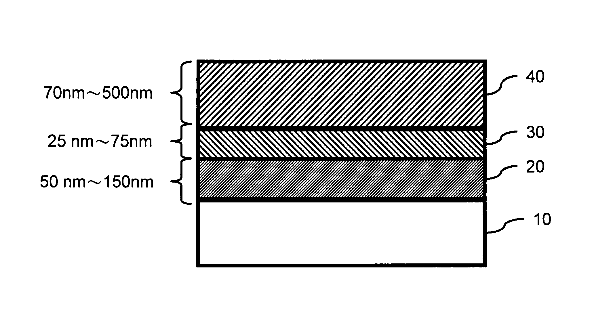
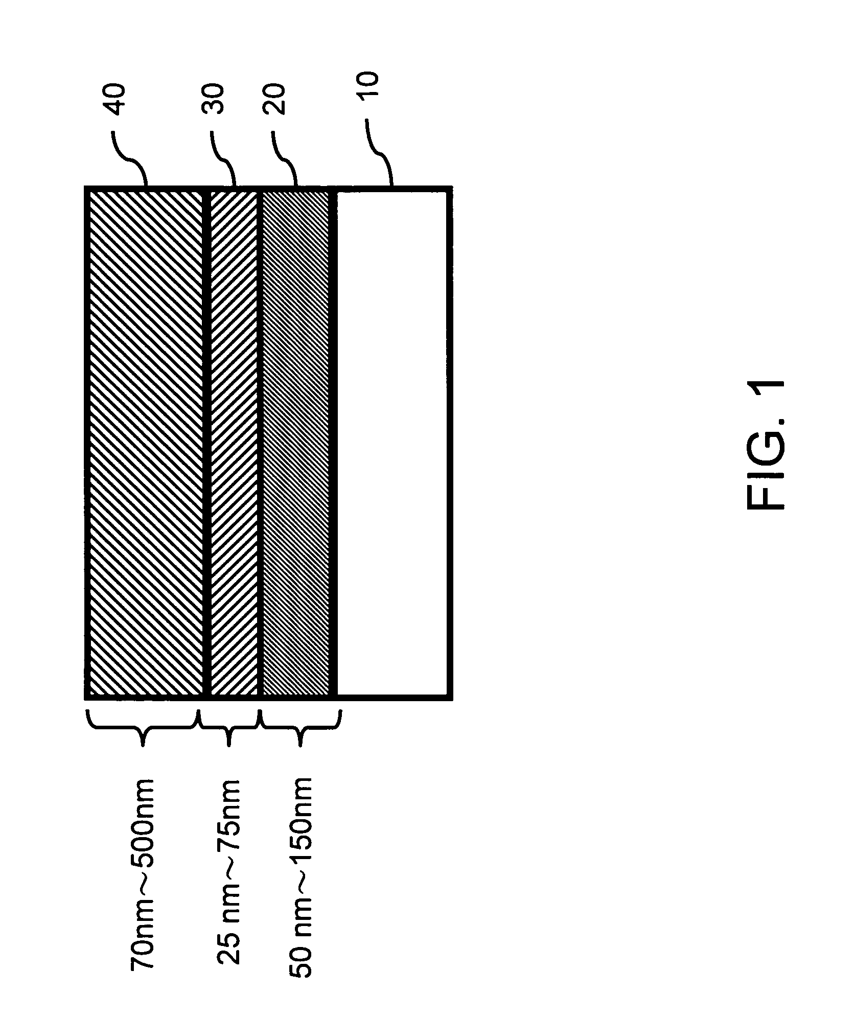
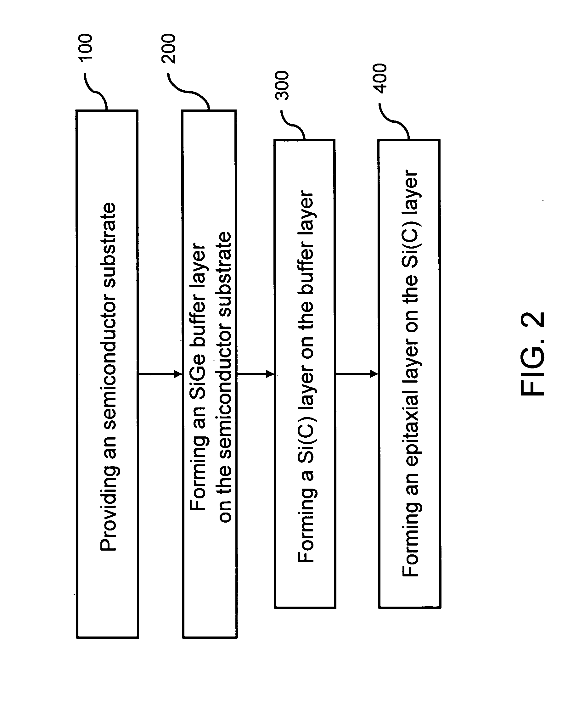
[0025]According the invention, a Si(C) layer is adopted to change the strain-relaxed mechanism of the SiGe epitaxial layer formed on the Si(C) layer. Refer to FIG. 1 illustrating the schematic construction. The construction includes a semiconductor substrate 10, the preferred embodiment, which is a Si substrate, a buffer layer 20 with a thickness of 50 nm to 150 nm formed on the semiconductor substrate 10, a Si(C) layer 30 with thickness of 25 nm to 75 nm formed on the buffer layer 20, and a SiGe epitaxial layer (Si1−xGex) 40 with thickness of 70 nm to 500 nm formed on the Si(C) layer 30. The lattice of the SiGe epitaxial layer 40 is different from that of the SiGe buffer layer 20. The thickness of the layers may be adjusted according to different need.

[0026]The Si(C) layer 30 is a heterostructure alloy mixed by VI family elements. The Si(C) layer 30 changes the strain mechanism of the SiGe epitaxial layer 40 such, that the SiGe epitaxial layer 40 has the characteristic of high stra...


PUM


Abstract

A construction of thin strain-relaxed SiGe layers and method for fabricating the same is provided. The construction includes a semiconductor substrate, a SiGe buffer layer formed on the semiconductor substrate, a Si(C) layer formed on the SiGe buffer layer, and an relaxed SiGe epitaxial layer formed on the Si(C) layer. The Si(C) layer is employed to change the strain-relaxed mechanism of the relaxed SiGe epitaxial layer formed on the Si(C) layer. Therefore, a thin relaxed SiGe epitaxial layer with low threading dislocation density, smooth surface is available. The fabricating time for fabricating the strain-relaxed SiGe layers is greatly reduced and the surface roughness is also improved.

Description

BACKGROUND OF THE INVENTION[0001]This Non-provisional application claims priority under 35 U.S.C. § 119(a) on Patent Application No. 093103814 filed in Taiwan on Feb. 17, 2004, the entire contents of which are hereby incorporated by reference.[0002]1. Field of Invention[0003]The present invention relates to a construction of strain-relaxed SiGe layers and method for fabricating the same, and more particularly to a construction of thin strain-relaxed SiGe layers and method for fabricating the same for strained Si using SixC1-x as insert layers.[0004]2. Related Art[0005]The semiconductor and integrated circuit technology has been developed in recent years, to be compact with high operation speed. How to increase the operation speed of the semiconductor device with lower power consumption constitutes an important issue in the very large scale integration (VLSI) field.[0006]Researches on SiGe material have shown that when a composite layer of Si and Ge is grown on a silicon substrate an...

Claims


Application Information

Patent Timeline
Patent Type & Authority Patents(United States)
IPC IPC(8): H01L29/06H01L21/20H01L29/10H01L29/165
CPCH01L21/02381H01L21/02447H01L21/0245H01L29/165H01L21/02532H01L29/1054H01L21/02502
Inventor CHEN, PANG-SHIULEE, SHENG-WEILIAO, KAO-FENGCHEN, LIH-JUANNLIU, CHEE-WEE
Owner IND TECH RES INST
Why Eureka
Try Eureka