Current sensing structure for integrated power switches

a current sensing structure and power switch technology, applied in the direction of ac-dc conversion, electric variable regulation, instruments, etc., can solve the problems of reducing efficiency and inaccuracy, and achieve the effect of stabilizing current and stabilizing curren

Active Publication Date: 2007-04-10
DIALOG SEMICONDUCTOR GMBH
View PDF7 Cites 16 Cited by
  • Summary
  • Abstract
  • Description
  • Claims
  • Application Information

AI Technical Summary

Benefits of technology

[0011]A principal object of the present invention is to sense the current through a coil of an integrated switching converter without the power losses caused by a resistor.
[0012]Another principal object of the present invention is to achieve a method for a fast and precise measurement of the current through the coil of an integrated switching converter.
[0015]In accordance with the objects of this invention a method to sense the current through an inductor of an integrated boost converter using an NMOS pass device has been achieved. The method invented comprises, firstly, to provide a circuitry having four branches, wherein a first branch is conducting the current to be measured, a second branch comprises at least one PMOS transistor, one NMOS transistor, and an NMOS pass device, wherein said current to be measured is flowing through said NMOS pass device and wherein the current through said at least one PMOS transistor and at least one NMOS transistor of the second branch is negligible small compared to the current to be measured, a third branch comprises the same number and type of transistors as said second branch and an NMOS device, wherein each of said transistors of the third branch is forming a current mirror with a correspondent transistor of the second branch and wherein said NMOS device is a replica of the NMOS pass device of the second branch having an n-times smaller size than said NMOS pass device and wherein both said NMOSFET devices are forming a current mirror, and a fourth branch comprises another PMOS transistor conducting the output current of the current sensing system wherein said PMOS transistor of the fourth branch is forming a current mirror with one correspondent transistor of each the third and second branch. The following steps of the method are to mirror the current through said NMOS pass device to said NMOS device of the third branch being a replica of said NMOS pass device, to stabilize the current of said third branch quickly by mirroring this current to the second branch and mirroring back from the second branch to the third branch wherein the current through the current mirror transistors of the second branch is negligible small compared to the current through said NMOS pass device, to mirror the current of the third branch to said PMOS transistor of said fourth branch, and to use the current of the fourth branch as a linearly correlated measure of the current to be measured of the first branch.
[0016]In accordance with the objects of this invention a method to sense the current through an inductor of an integrated buck converter using a PMOS pass device has been achieved. The method invented comprises, firstly, to provide a circuitry having four branches, wherein a first branch is conducting the current to be measured, a second branch comprises at least one PMOS transistor, one NMOS transistor, and a PMOS pass device, wherein said current to be measured is flowing through said PMOS pass device and wherein the current through said at least one PMOS transistor and at least one NMOS transistor of the second branch is negligible small compared to the current to be measured, a third branch comprises the same number and type of transistors as said second branch and a PMOS device, wherein each of said transistors of the third branch is forming a current mirror with a correspondent transistor of the second branch and wherein said PMOS device is a replica of the PMOS pass device of the second branch having an n-times smaller size than said PMOS pass device and wherein both said PMOSFET devices are forming a current mirror, and a fourth branch comprises another NMOS transistor conducting the output current of the current sensing system wherein said NMOS transistor of the fourth branch is forming a current mirror with one correspondent transistor of each the third and second branch. The following steps of the method invented are to mirror the current through said PMOS pass device to said PMOS device of the third branch being a replica of said PMOS pass device, to stabilize the current of said third branch quickly by mirroring this current to the second branch and mirroring back from the second branch to the third branch, wherein the current through the current mirror transistors of the second branch is negligible small compared to the current through said PMOS pass device, to mirror the current of the third branch to said NMOS transistor of said fourth branch, and to use current of the fourth branch as a linearly correlated measure of the current to be measured of the first branch.

Problems solved by technology

Using resistor R for current I0 sensing introduces inaccuracies, especially when integrated on chip, and reduces efficiency.

Method used


Image

  • Current sensing structure for integrated power switches
  • Current sensing structure for integrated power switches
  • Current sensing structure for integrated power switches

Examples


Embodiment Construction

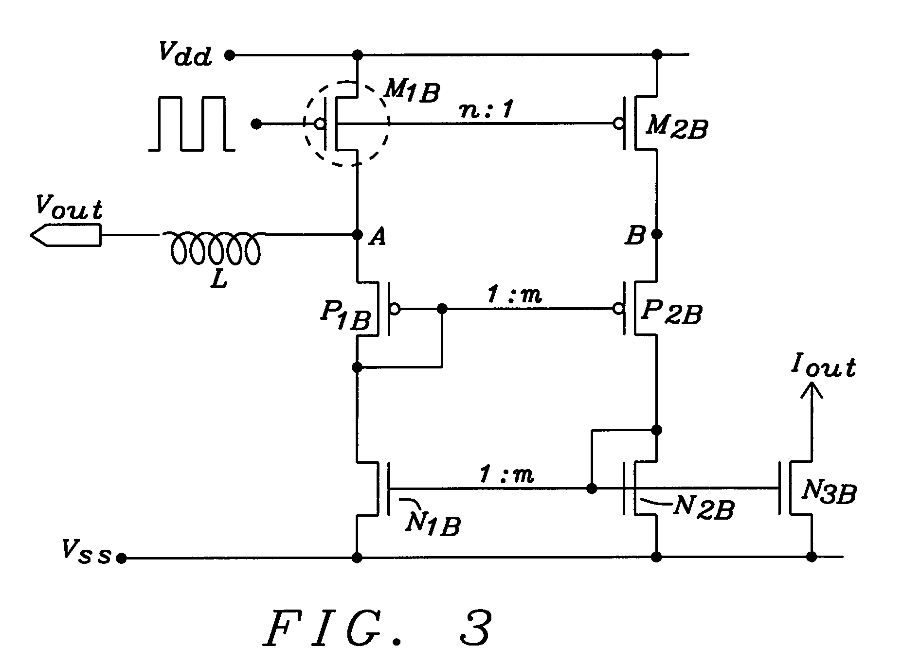
[0023]The preferred embodiments of the present invention disclose novel circuits and methods used for current sensing of integrated switching converters. It has to be understood that the structure of the circuits could be used for a multitude of different current sensing applications.

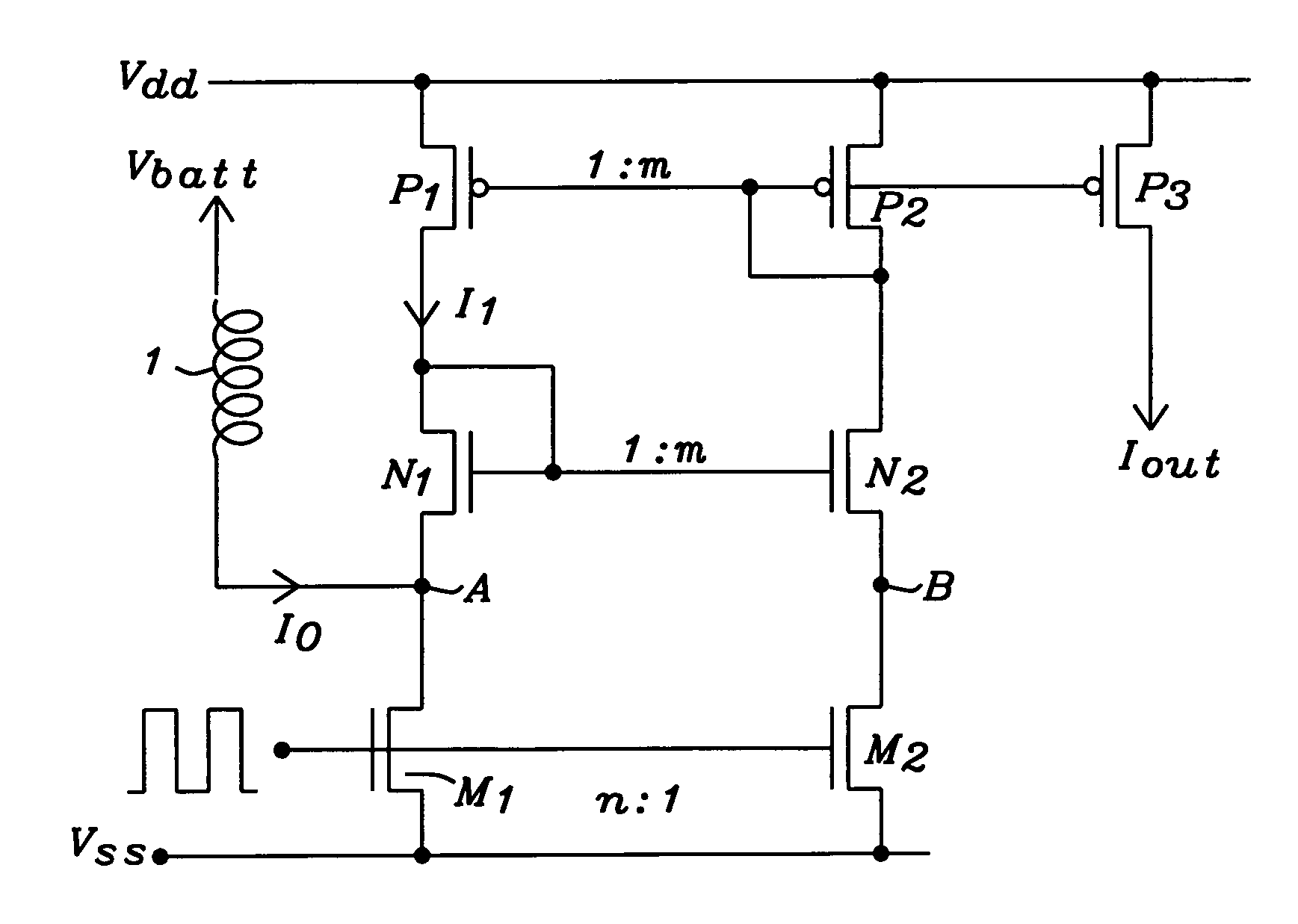
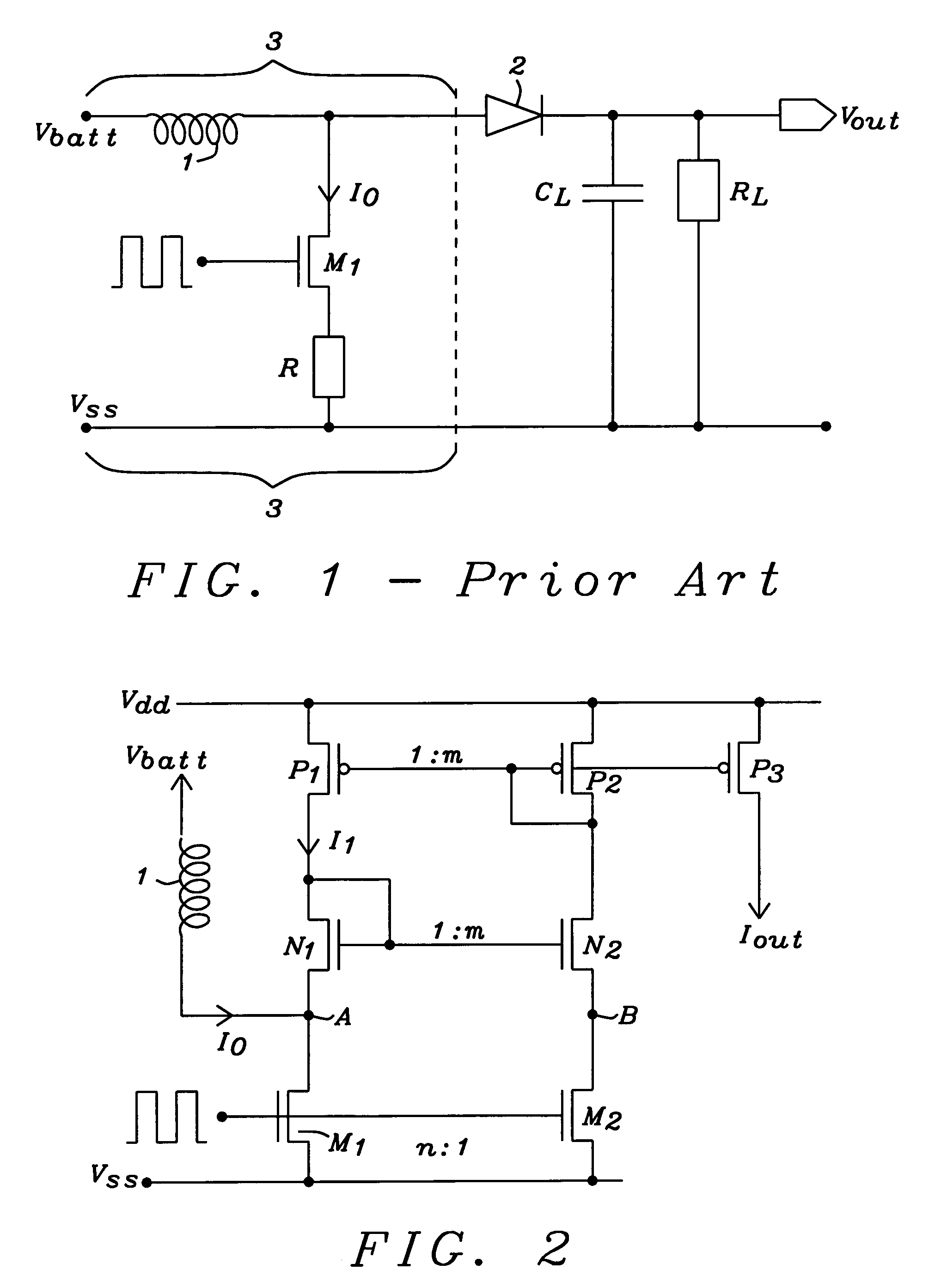
[0024]FIG. 2 shows, as example of the circuit invented, a schematic of the switching and current sensing part of an integrated switching boost converter. The invention uses a “replica biasing” technique to avoid a resistor for current measurement as shown in FIG. 1 prior art. In the circuit shown in FIG. 2 the current through the pass device M1 is sensed by biasing another MOSFET device M2 under similar conditions like pass device M1 but with scaled dimensions. Similar conditions mean in this context that gate, source and drain voltages of pass device and MOSFET device M2 are nearly equal. In the case of the present invention the gate and source connections are identical anyway and the self-biased loop ...


PUM


Abstract

Circuits and methods to sense the current through a coil of an integrated switching converter, applicable to boost and to buck converters, have been achieved. The present invention uses a “replica biasing” technique to avoid a resistor for current measurement. The current through a pass device is mirrored into a replica, having a scale of n and being much smaller in size, of said pass device. The current through the replica is mirrored to another branch of the circuit and back again to achieve a fast stabilization of the current. The current through the replica is mirrored again to an output branch of the circuit, which conducts exactly a fraction 1 / n of the current flowing through the pass device. The self-biasing current loop of the invention adapts quickly to the actual current level through the pass device of the switching converter. Accuracies better than 5% are achieved over a wide range of dynamic range.

Description

BACKGROUND OF THE INVENTION[0001](1) Field of the Invention[0002]The invention relates to electrical power supplies, and more particularly to sensing the current through coils of switching regulators as e.g. boost or buck converters.[0003](2) Description of the Prior Art[0004]Integrated switching regulators as e.g. boost or buck converters usually have a current control loop requiring accurate sensing of the actual current through an external coil during operation. Usually a small resistor is therefore connected in series to a large MOSFET switch, which conducts this current during on state. FIG. 1 prior art shows a schematic of such a conventional prior art configuration using an NMOS switch. The circuit of FIG. 1 comprises an external coil 1, a large MOSFET switch M1, a sense resistor R, a diode 2, and a capacitor CL and a resistor RL, both representing a load. The part 3 on the left side represents the inductor and the current sense function of the integrated switching converter....

Claims


Application Information

Patent Timeline
Patent Type & Authority Patents(United States)
IPC IPC(8): G01R31/26
CPCH02M3/156H02M2001/0009H02M1/0009
Inventor EBERLEIN, MATTHIAS
Owner DIALOG SEMICONDUCTOR GMBH
Why Eureka
Try Eureka