Hermetically sealed microdevice with getter shield

a technology of getter shield and micro-device, which is applied in the manufacture of electric discharge tubes/lamps, electrical devices, and electrical systems, etc., can solve the problems of difficult manufacturing and expensive production, prone to pressure increase in vacuum sealed cavities, and operational problems

Inactive Publication Date: 2007-04-17
TEMIC AUTOMOTIVE OF NORTH AMERICA
View PDF15 Cites 69 Cited by
  • Summary
  • Abstract
  • Description
  • Claims
  • Application Information

AI Technical Summary

Problems solved by technology

Considering the variety of devices, one feature many of these devices have in common is complex structures that must be contained in separate hermetic packaging, which can be difficult to manufacture and expensive to produce.
In addition to packaging issues, there are operational issues.
A vacuum-sealed cavity is typically susceptible to pressure increases due to gas generation during the hermetic sealing process and outgassing from the package material, sealing material, and components within the cavity.
This pressure variation can degrade device performance and reduce device lifetime for many hermetically sealed microdevices.
In addition, the packaging and / or equipment to provide an evacuated package can be complex and expensive.
For instance, with thick film getters there can be a reliability issue caused by getter particles falling down during fabrication process or after device experiencing vibration or shock due to poor mechanical strength and too large pore size of the used getter.
The presence of separated getter particles has been identified as a major failure mode for some micro gyroscopes sealed with porous thick film getters.
Additionally, because conventional getters typically have large pore size, the required size of the getter is normally large.
With relation to thin film getters, the mechanical properties of known amorphous or poly-crystalline silicon will change with deposition condition and are difficult to repeat.

Method used


Image

  • Hermetically sealed microdevice with getter shield
  • Hermetically sealed microdevice with getter shield
  • Hermetically sealed microdevice with getter shield

Examples


Embodiment Construction

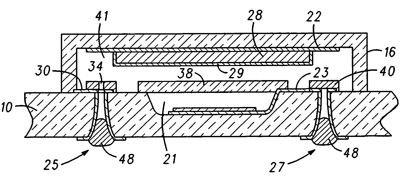
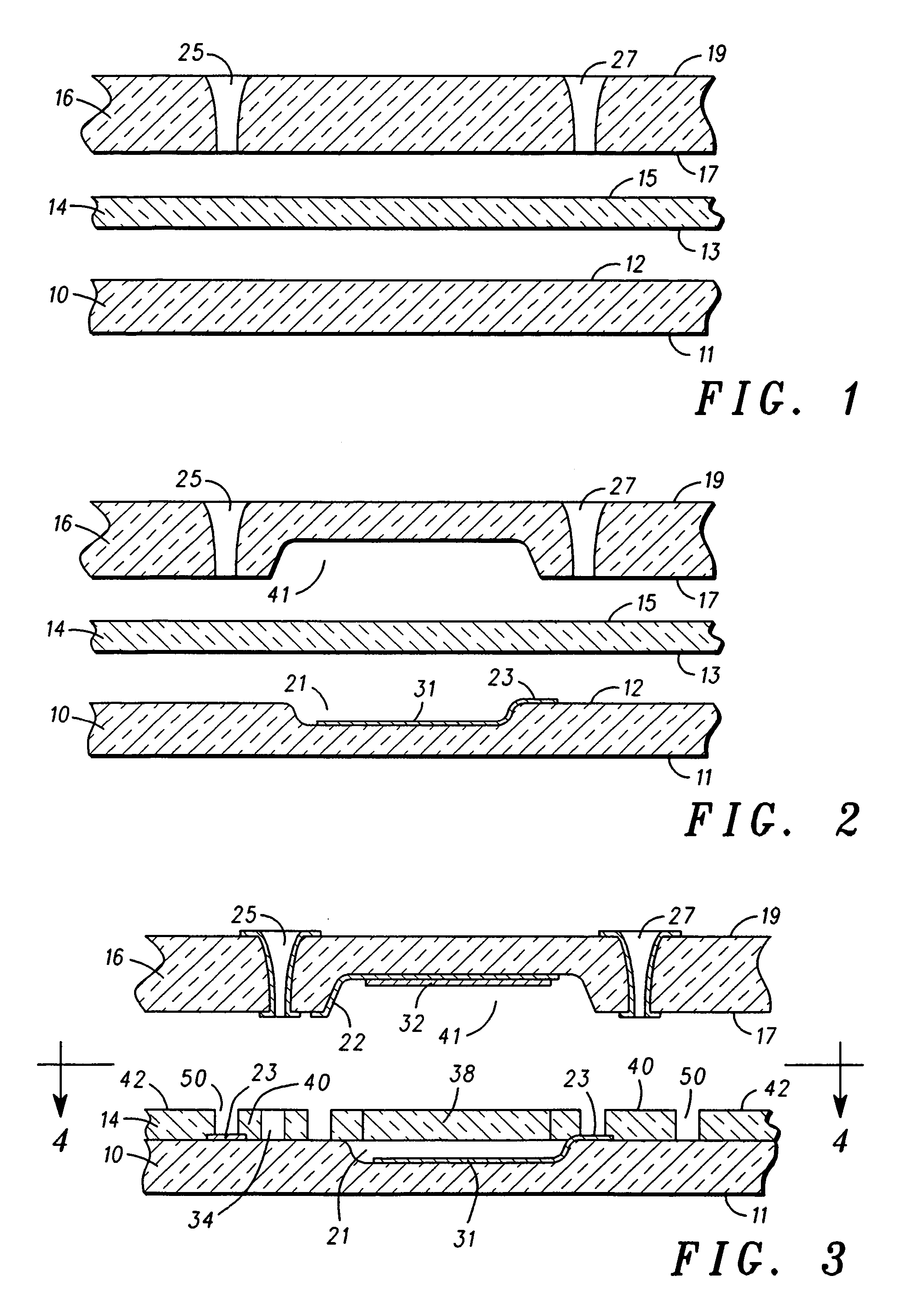
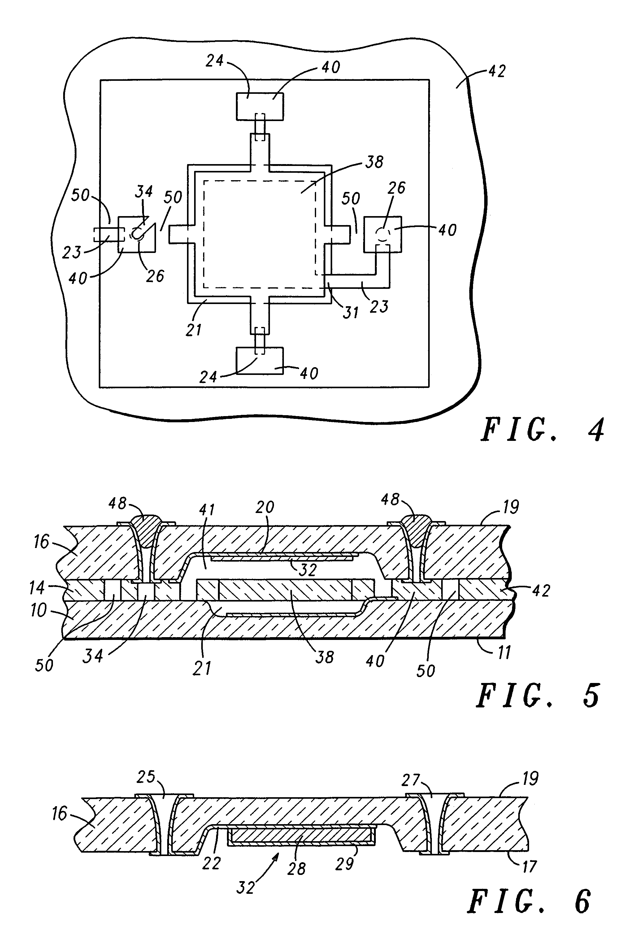
[0016]The present invention is a packaging assembly for a microdevice and method therefor, which can provide a vacuum environment for the microdevice under a hermetic seal. The microdevice is provided in a simple assembly at a low cost and with a high reliability. In particular, the present invention provides a simple assembly structure that can be easily evacuated and hermetically sealed. Specifically, a vent channel is integrated in the same silicon wafer, and processed at the same time, when constructing the actual microdevice. Preferably, a metallic getter is incorporated into the package to maintain the vacuum, particularly in view of the various higher temperature sealing processes that can cause outgassing within the package. More preferably, the metallic getter is also used as an electrical shield and / or ground.

[0017]For purposes of illustration and description, an example of a micro gyroscope will be used as the microdevice. However, the present invention is not limited to ...


PUM


Abstract

A microdevice that comprises a device microstructure (38) and vent channel (34) in a wafer (14) that is sandwiched between a substrate (10) and a cap (16). The cap (16) and substrate (10) have recesses (41, 21) around the microstructure (22) to define a cavity. A vent (25) is connected to the vent channel (34) and subsequently to the cavity. The vent (25) is used to evacuate and seal the microstructure (38) in the cavity. A getter layer (32) can be used to maintain the cavity vacuum. An electrical connection can be provided through the vent (25), vent channel (34) and cavity to the getter (32) to electrically ground the getter layer (32).

Description

FIELD OF THE INVENTION[0001]This invention in general relates to microdevices having a structure that requires a vacuum cavity and, more particularly, to a microdevice and procedure for making a microdevice having a hermetically sealed vacuum in the cavity surrounding the microdevice.BACKGROUND OF THE INVENTION[0002]Microdevices having bonded conductive and insulating substrates can be fabricated with many different materials. A combination of metal, glass, and semiconductor materials are often used to create these devices and their packages. These materials are fused into a structure by many different processes as are known in the art. Some of these devices require a sealed chamber with a device therein and electrical connections to outside the package. There are very many microdevices that typically have a requirement for this type of structure. Considering the variety of devices, one feature many of these devices have in common is complex structures that must be contained in sepa...

Claims


Application Information

Patent Timeline
Patent Type & Authority Patents(United States)
IPC IPC(8): H01J9/00B81C99/00
CPCB81B7/0038B81B7/007
Inventor DING, XIAOYIFRYE, JEFFREY J.SCHUSTER, JOHN P.
Owner TEMIC AUTOMOTIVE OF NORTH AMERICA
Why Eureka
Try Eureka