Routing design to minimize electromigration damage to solder bumps

a technology of flip chip and bump, which is applied in the direction of semiconductor devices, electrical equipment, and semiconductor/solid-state device details, etc., can solve the problems of high current density in the bump, loss of continuity, and failures that are premature, so as to reduce current crowding, reduce the damage of the solder bump, and reduce the effect of current density

Active Publication Date: 2007-04-24
AVAGO TECH INT SALES PTE LTD
View PDF10 Cites 26 Cited by
  • Summary
  • Abstract
  • Description
  • Claims
  • Application Information

AI Technical Summary

Benefits of technology

[0014]A novel pad structure and current routing design for pads of an integrated circuit component are described in detail hereinafter. The pad structure of the invention includes a first pad implemented on an inner conductive layer of an integrated circuit component, a second pad implemented on an outer conductive layer of the integrated circuit, and a plurality of vias each directly connecting the inner pad to the outer pad. A current delivering trace is connected to the first pad. The second, or “outer”, pad is sealed around its edges with a passivation layer, which includes an opening exposing the conductive outer pad. The exposed area of the conductive outer pad is hereinafter referred to as the “pad opening”. The vias connecting the inner pad to the outer pad are positioned within the footprint of the pad opening. Thus, as current is delivered to the inner pad from the trace, the via impedances, which are each higher than the impedance of the current delivering trace, causes the current to divide and flow to the outer pad over the plurality of vias, thus distributing the current and reducing current crowding at the inner pad. At a minimum this results in a reduction in the maximum current density seen on the outer pad, and therefore a reduction in electromigration damage in the solder bump caused by current crowding. With a small amount of additional planning with regards to the selection of the number and layout of the vias connecting the inner and outer pads within the footprint of the pad opening, the current flow to the outer pad can be optimized to produce a relatively uniform current density.

Problems solved by technology

Electromigration can cause the complete depletion of material within a conductor leading to the loss of continuity.
Electromigration is a problem commonly seen in high-current-flow bumps of flip-chip assemblies, so named because during formation, the die pads are formed on the top layer of the integrated circuit die, bumps are added, and the die is then “flipped” over and connected directly to the chip substrate via the bumps.
High local values of the current density, J, may cause failures that are premature in time when compared with the failures that occur when the current is uniformly distributed in the bump 16.
Thus, future bumps may have smaller cross-sections, leading to the problem of higher current densities in the bumps.

Method used


Image

  • Routing design to minimize electromigration damage to solder bumps
  • Routing design to minimize electromigration damage to solder bumps
  • Routing design to minimize electromigration damage to solder bumps

Examples


Embodiment Construction

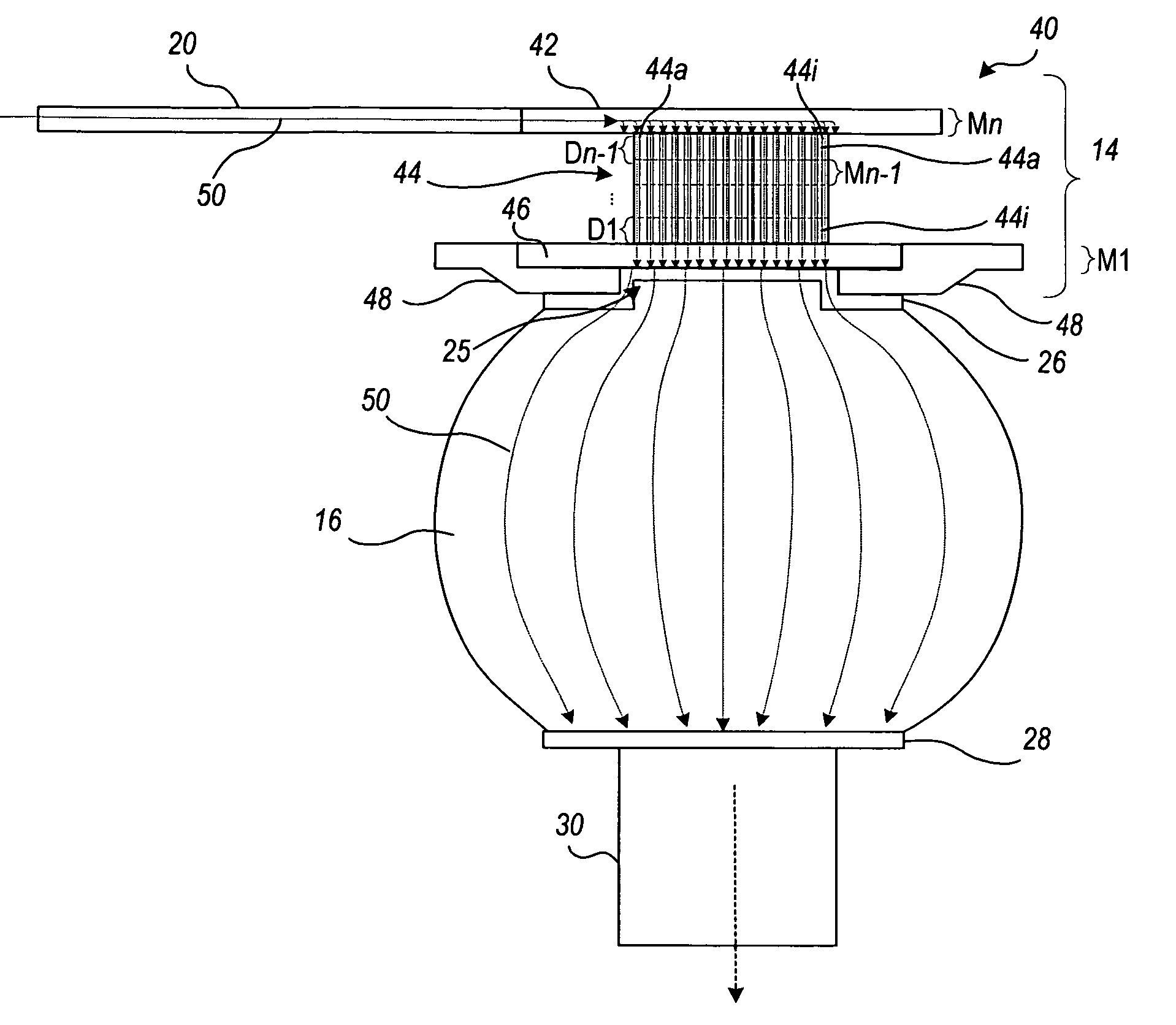
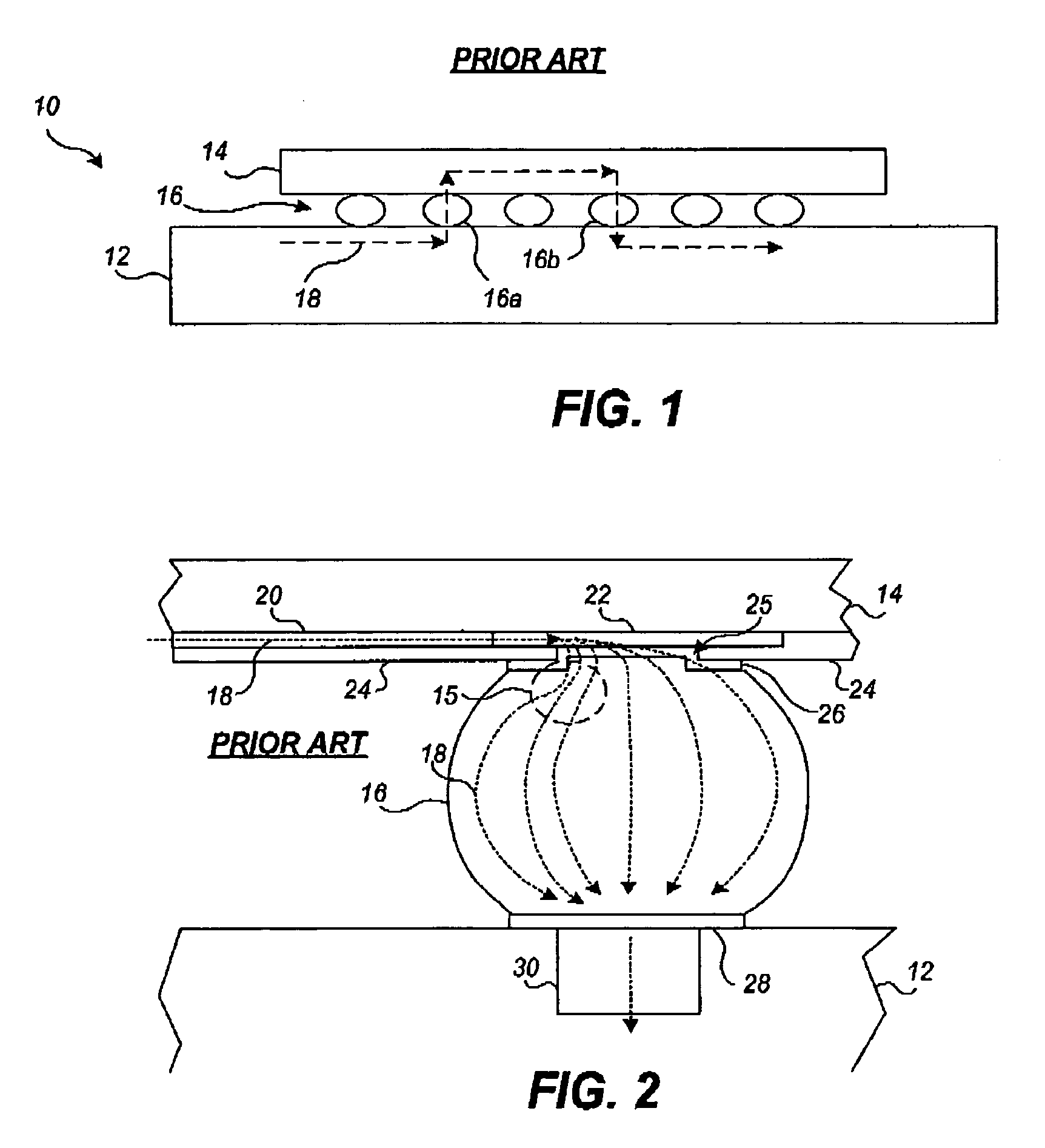
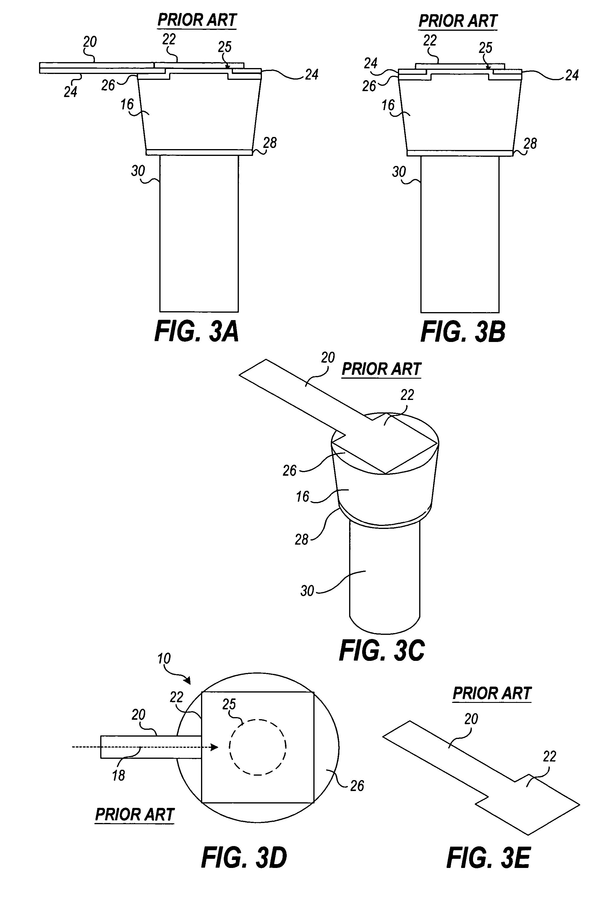
[0028]A novel design for integrated circuit component pads is described in detail below that seeks to achieve a reasonably uniform current distribution on the outer pad interface to assist in reducing electromigration damage in a joint (e.g., flip-chip bump) connected to the pad. For purposes of comparison, the configuration of a traditional prior art solder bump in a flip-chip assembly is shown in FIGS. 3A, 3B, 3C, 3D, and 3E. More particularly, FIG. 3A is a cross-sectional side view, FIG. 3B is a cross-sectional front view, FIG. 3C is an isometric view, and FIG. 3D is a top plan view of the components included in a single bump junction of the flip-chip assembly 10 of FIG. 1. FIG. 3E is a perspective view of the trace 20 and pad 22 of FIGS. 3A–3D. As illustrated in FIGS. 3A, 3B, 3C, and 3D, the trace 20 is conductively connected to the pad 22 on the outermost trace layer of the integrated circuit 14 (of FIG. 1). The pad 22 is capped with a passivation layer 24, typically comprising...


PUM


Abstract

A novel pad structure for an integrated circuit component that utilizes a bump interconnect for connection to other integrated circuit components that produces a relatively uniform current distribution within the bump of the bump interconnect is presented. The pad structure includes an inner pad implemented on an inner conductive layer of the integrated circuit component, an outer pad implemented on an outer conductive layer of the integrated circuit component, and a plurality of vias connecting the inner pad and outer pad. The outer pad is sealed preferably around its edges with a passivation layer, which includes an opening exposing a portion of the outer pad. The vias connecting the inner pad and outer pad are preferably implemented to lie in a via region within the footprint of the pad opening.

Description

BACKGROUND OF THE INVENTION[0001]The present invention relates generally to flip chip packaging technologies for integrated circuits more particularly to a methodology and trace design for minimizing electromigration damage to integrated circuit connection joints such as solder bumps in a flip-chip assembly.[0002]Electromigration is the movement of material within a conductor that is caused by the flow of electrical current. Electromigration can cause the complete depletion of material within a conductor leading to the loss of continuity. The effect is more apparent at interconnect junctions, for example, in a solder bump connecting a flip-chip die and substrate, and is dependent on the current density (higher being worse than lower), the material (some materials resisting the effects of electromigration more than others), and the geometry of the structure.[0003]Electromigration is a problem commonly seen in high-current-flow bumps of flip-chip assemblies, so named because during fo...

Claims


Application Information

Patent Timeline
Patent Type & Authority Patents(United States)
IPC IPC(8): H01L23/48H01L23/52H01L29/40
CPCH01L24/11H01L24/05H01L24/13H01L2224/13099H01L2924/01015H01L2924/01025H01L2924/01033H01L2924/0105H01L2924/01078H01L2924/01082H01L2924/01322H01L2924/014H01L2924/14H01L2924/3011H01L2924/0002H01L2224/0401H01L2924/0001H01L2224/131H01L2224/05572H01L2224/13006H01L2924/01006H01L2224/05552H01L23/12
Inventor RICHLING, WAYNE PATRICKDAUKSHER, WALTER JOHNGRAUPP, WILLIAM S.
Owner AVAGO TECH INT SALES PTE LTD
Why Eureka
Try Eureka