Method and apparatus for driving passive matrix liquid crystal

a passive matrix liquid crystal and liquid crystal technology, applied in the direction of instruments, computing, electric digital data processing, etc., can solve the problem of not being able to reduce the selection voltage with l=3, the complexity of the power source circuit is disadvantageous to the size of the driver circuit of the column electrode, and the need to realize the fine-processing with high voltage tolerance, etc. problem, to achieve the effect of low voltage, high contrast display and reduced power consumption

Inactive Publication Date: 2007-04-24
KAWASAKI MICROELECTRONICS
View PDF23 Cites 4 Cited by
  • Summary
  • Abstract
  • Description
  • Claims
  • Application Information

AI Technical Summary

Benefits of technology

[0033]In view of the above conventional problems, the present invention has a first object of providing multiline addressing drive method and apparatus for passive matrix liquid crystal, capable of preventing the occurrence of a frame response phenomenon of high-speed liquid crystal while realizing the high contrast display, the driving at a low voltage, the reduced power consumption and the reduction in chip size.
[0034]In view of the above conventional problems, the present invention has a second object of providing a drive method and a liquid crystal driving apparatus for passive matrix liquid, capable of displaying a letter, a slow motion picture, or a static picture at multi-gradation levels in passive matrix liquid crystal such as STN liquid crystal and of restraining the drop in contrast, the increase in power consumption, the splicing, and the reduction in color reproducibility to display a multi-gradation full motion picture.
[0035]In view of the above conventional problems, the present invention has a third object of providing multiline addressing (MLA) drive method and apparatus for passive matrix liquid, capable of eliminating the brightness unevenness generated in a horizontal direction, which is peculiar to the MLA drive system, so as to improve the display quality of an LCD, in the MLA drive system for simultaneously driving a plurality of rows of passive matrix liquid crystal by using an orthogonal function.

Problems solved by technology

However, the area of a display data memory is increased along with the improvement in colorization, resulting in a dilemma that a fine-process with high voltage tolerance should be realized.
For example, the above-mentioned conventional LCD driving systems have the following problems.
As a result, a power source circuit is complicated to disadvantageously increase the size of a driver circuit of the column electrodes.
However, the selection voltage cannot be lowered with L=3.
In this manner, this drive system is not suitable for a fine-process for its high selection voltage, and therefore is not useful for mounting a driver circuit on one chip.
Thus, there is a problem in that the BLA3 drive system is also no more suitable for applications such as a portable telephone.
Accordingly, higher speed is required, leading to increased power consumption.
As a result, there arises a problem in that the LCD panel cannot respond to such a high frequency.
Therefore, there are problems that a column signal has similarly a higher frequency and that a column selection time period is gradually reduced.
Since the high-speed driving is performed in the motion picture display as described above, there is a problem that the contrast is disadvantageously lowered due to the frame response phenomenon.
However, the same problem arises for a higher frequency.
There is a problem in that the presence of a plurality of chips increases the cost.
Furthermore, the MLA drive system has a problem in that the brightness unevenness is generated in a horizontal direction.
On the other hand, the column voltage control disclosed in the above-mentioned JP 11-24637 A does not serve as an effective solution for the horizontal brightness unevenness.
Therefore, if it is intended to predict a series of column voltage sequences over frames so as to determine whether the column voltage is to be increased or not, the circuit is extremely complicated.
Thus, such a solution is not practical.
In this case, however, the brightness unevenness appears in a direction of the column electrode (normally, in a longitudinal direction).
Although the reason for occurrence of the horizontal brightness unevenness is not elucidated, it is supposed that such brightness unevenness is caused due to optical response characteristics depending on a pattern of a row electrode voltage and a column electrode voltage applied to liquid crystal in time sequence.
Therefore, the above-mentioned related art cannot solve the problem of the horizontal brightness unevenness.

Method used


Image

  • Method and apparatus for driving passive matrix liquid crystal
  • Method and apparatus for driving passive matrix liquid crystal
  • Method and apparatus for driving passive matrix liquid crystal

Examples


first embodiment

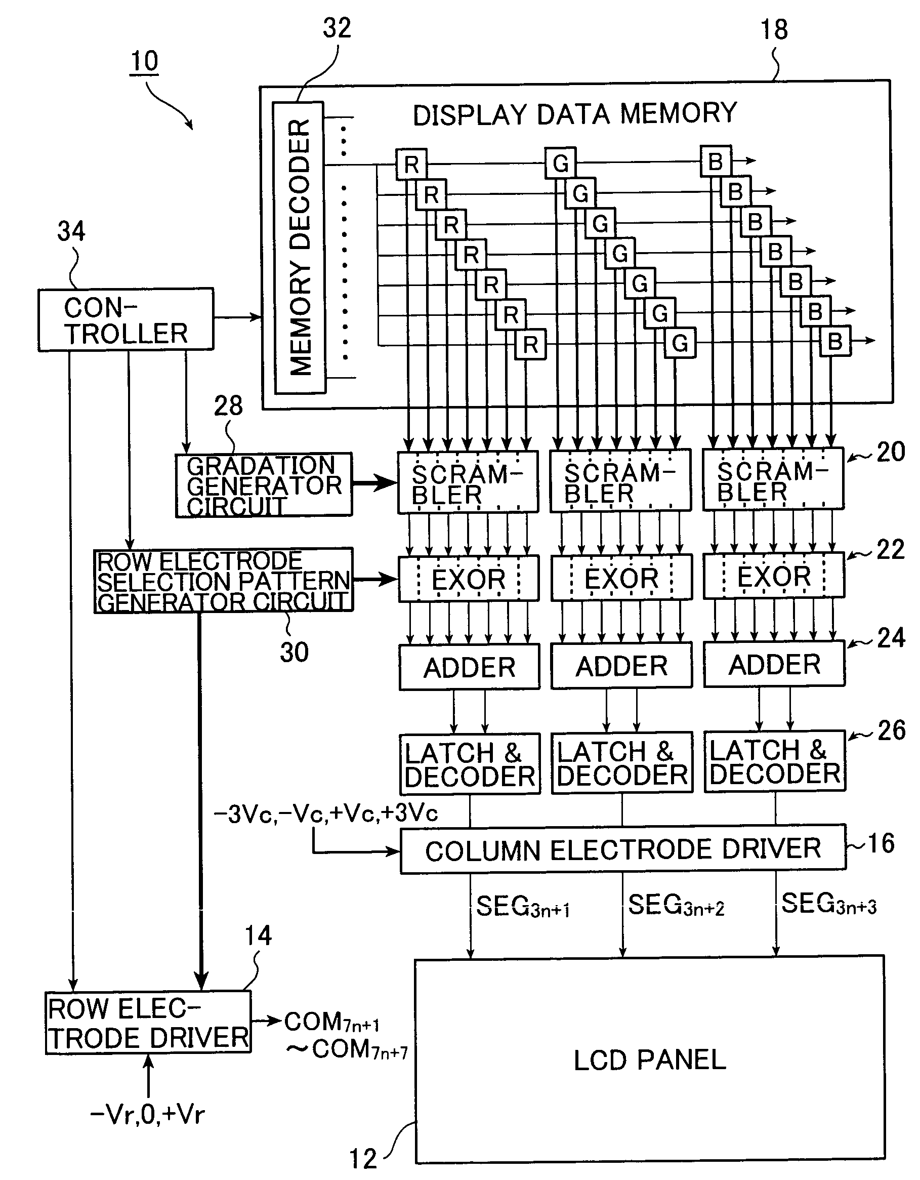
[0093]FIG. 1 is a block diagram showing a circuit configuration of an embodiment (first embodiment) of a liquid crystal driving apparatus (LCD driver) for implementing a multiline addressing drive method for passive matrix liquid crystal according to a first mode of the present invention. The LCD driver according to this embodiment selects 7 row electrodes at a time and sets four voltage levels for the column electrodes. In the present invention, this drive method is referred to as an FLA7 (Four-Level Addressing 7) drive system.

[0094]As shown in FIG. 1, an LCD driver 10 of this embodiment employs the MLA drive system for simultaneously selecting seven rows (COMMON) from row electrodes on an LCD panel 12 and driving the LCD panel at four voltage levels of the column electrodes. The LCD driver includes a row electrode driver 14, a column electrode driver 16 and a display data memory (for example, RAM) 18.

[0095]The LCD driver also includes, for each column (segment) of each color of RG...

second embodiment

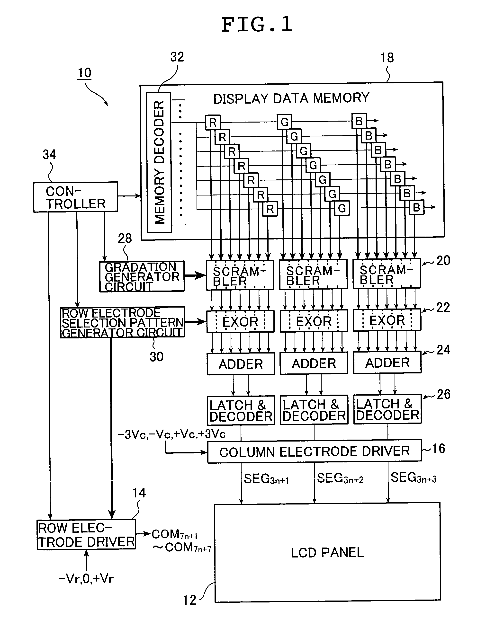
[0148]Next, the first mode of the present invention will be described.

[0149]FIG. 5 is a block diagram showing a circuit configuration of another embodiment (second embodiment) of a liquid crystal driving apparatus (LCD driver) for implementing a multiline addressing drive method for passive matrix liquid crystal according to the present invention. The LCD driver according to this second embodiment simultaneously selects eleven row electrodes and has six voltage levels of the column electrodes. In the present invention, this drive method is referred to as SLA11 (Six-Level Addressing 11). An LCD driver 110 shown in FIG. 5 basically has a structure similar to that of the LCD driver 10 shown in FIG. 1 except that the number of simultaneously selected row electrodes is 11 instead of 7, the number of voltage levels of the column electrodes is 6 instead of 4, and only one scrambler, EXOR, adder and latch and decoder are provided because RGB are respectively processed in time division inste...


PUM


Abstract

A method and an apparatus for driving passive matrix liquid crystal, comprising the steps of: simultaneously selecting Y row electrodes, where Y is an odd number of 7 and above; calculating an exclusive OR between a Y-bit row selection vector representing a selection pattern of the Y row electrodes and Y-bit ON / OFF display data representing a display pattern of column electrodes, for each corresponding bit; adding the exclusive ORs for each bit; when X=(Y+1) / 2, and a 1 / (X−1) voltage of the maximum voltage of the column electrodes is Vc, selecting a voltage level of the column electrodes from X voltage levels satisfying:[2×i−(X−1)]×Vc (i=an integer of 0 to (X−1)) in accordance with the result of the addition for driving. These method and apparatus prevent the frame response phenomenon of high-speed liquid crystal while realizing high-contrast display, low-voltage driving, low power consumption, and reduction in chip size.

Description

TECHNICAL FIELD[0001]The present invention relates to a method and a apparatus for driving passive matrix liquid crystal, in particular, to multiline addressing (MLA) drive method and apparatus for passive matrix liquid crystal, which employ an MLA drive system, a drive method and a liquid crystal driving apparatus for passive matrix liquid crystal, which employ an MLA drive system with the addition of an FRC (frame rate control) gradation system to a PWM (pulse width modulation) gradation system, to display a multi-gradation color motion picture on the passive matrix liquid crystal, and multiline addressing drive method and apparatus for passive matrix liquid crystal, which allow the elimination of horizontal brightness unevenness peculiar to an MLA drive system so as to enable high-quality display.BACKGROUND ART[0002]Conventionally, a liquid crystal display (hereinafter, referred to as LCD) has been used as a display apparatus for a word processor or a personal computer. Due to it...

Claims


Application Information

Patent Timeline
Patent Type & Authority Patents(United States)
IPC IPC(8): G09G5/00G09G3/20G09G3/36
CPCG09G3/3625G09G3/2014G09G3/2018G09G3/2025G09G3/2077G09G3/3692G09G2320/0233G09G2320/0247G09G2320/0261G09G2320/0613G09G2330/021G09G3/36
Inventor SAKO, NORIMITSUKITAYAMA, HIDEYUKI
Owner KAWASAKI MICROELECTRONICS
Why Eureka
Try Eureka