Level shifter and display device using same

a level shifter and display device technology, applied in the field of level shifters, can solve the problems of unnecessary power consumption, unnecessary power consumption, unnecessary power consumption, etc., and achieve the effect of reducing power consumption, reducing mobility, and effectively reducing the amount of power consumption

Active Publication Date: 2007-04-24
SHARP KK
View PDF8 Cites 17 Cited by
  • Summary
  • Abstract
  • Description
  • Claims
  • Application Information

AI Technical Summary

Benefits of technology

[0031]According to this arrangement, thanks to the operation of the operation control section, the stationary current flows in the level shifting section only during the period in which the start signal is on the active level, while the stationary current is cut off during the period in which the start signal is on the non-active level. On this account, the power consumption is reduced compared to the arrangement in which the stationary current always flows.
[0033]Furthermore, the operation change due to the change of the input signal occurs in the next shifting operation period of the shift register, after the period in which the change of the input signal occurs. For this reason, when the input signal changes, it is possible to cause the operation to follow the change with no time lag.
[0037]The drive circuits for driving data signal lines and scanning signal lines, the drive circuits being formed so as to be integral with the display panel and being made of polycrystalline silicon and the like have mobility lower than the mobility of external circuits made of single-crystal silicon chips. For this reason, the drive voltage of the drive circuits is higher than the drive voltage of the external circuits, and hence it is necessary to provide a level shifter to a drive circuit to which a signal is supplied from an external circuit. Using the shift register of the present invention makes it possible to effectively reduce the amounts of power consumption in the data signal line drive circuit, the scanning signal line drive circuit, and also the display device.
[0038]In addition to the reduction of the power consumption, the change of the input signal is not reflected during the shifting operation of the shift register, i.e. during the writing operation, image reproduction is performed with no defects, even if the input signal is a signal directly contributes to the image reproduction. Furthermore, the change of the input signal is reflected to the change in the image reproduction with no time lag.

Problems solved by technology

However, although such a stationary current is required for level-shifting the low-voltage input signal in to the high-voltage output signal out, the stationary current unnecessarily flows even when the level shifting is not carried out, thereby unnecessarily increasing the power consumption.
However, the shift direction is not frequently switched, and hence one of the level shifters is kept unused until the shift direction is changed.
This patent application found that, in Japanese Laid-Open Patent Application No. 2000-322020, the stationary current always flows in the level shifter being used and this current also results in unnecessary power consumption.
Therefore, unnecessary power consumption due to the above-described stationary current also occurs in this level shifter for the shifting direction switching signal.
This is because, if the shifting direction switching signal is changed during the signal shifting in the bi-directional shift register, the shifting direction is switched in the midst of the shifting operation, so that an image may not be properly reproduced.
The above-described problem of unnecessary power consumption in the level shifter for the shifting direction switching signal occurs not only in the level shifter for the shifting direction switching signal but also in level shifters for signals which are not frequently changed as in the case of the shifting direction, such as a resolution switching signal for switching resolutions and a driver switching signal for switching between a binary driver and an analog driver.

Method used


Image

  • Level shifter and display device using same
  • Level shifter and display device using same
  • Level shifter and display device using same

Examples


Embodiment Construction

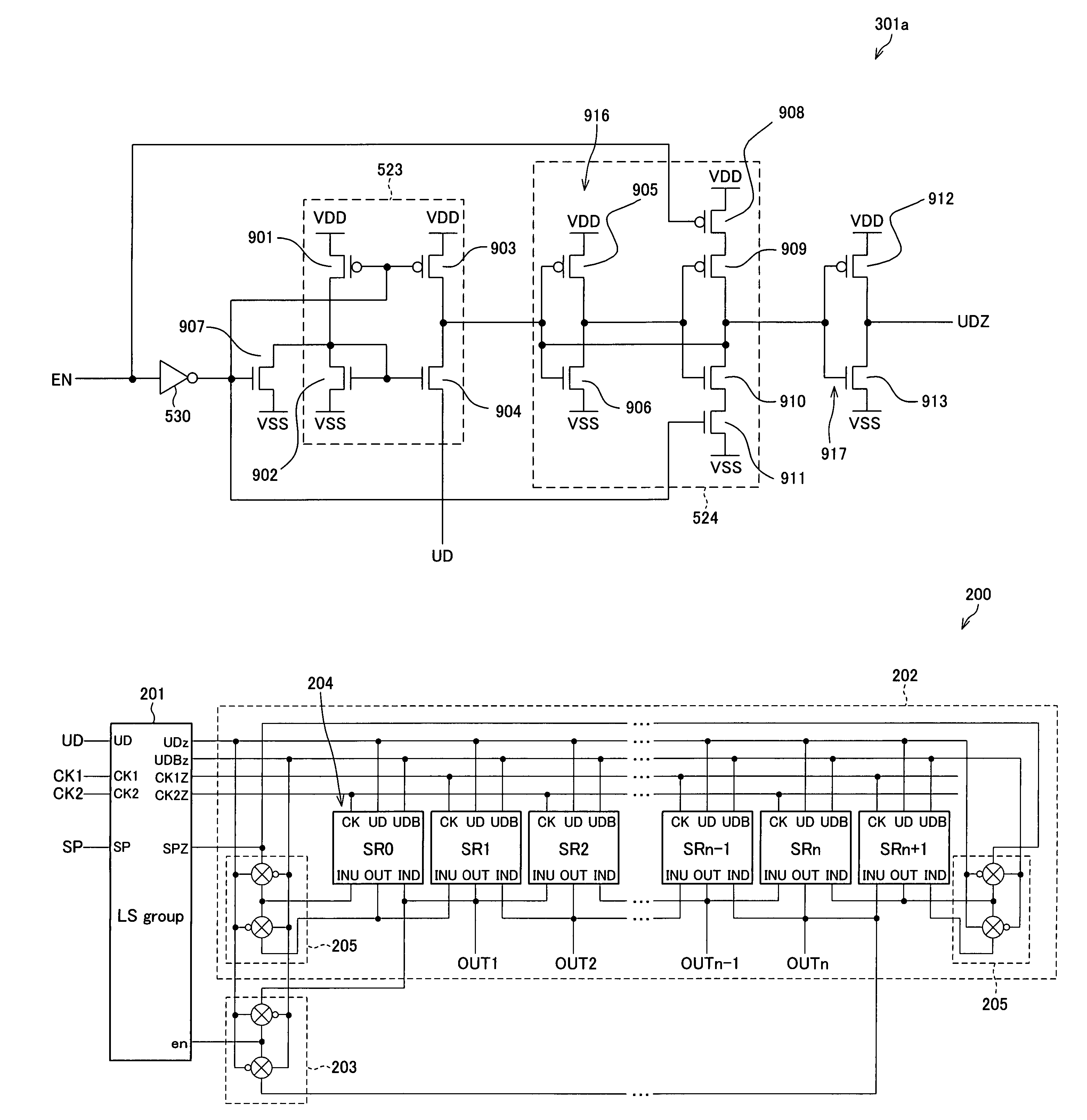
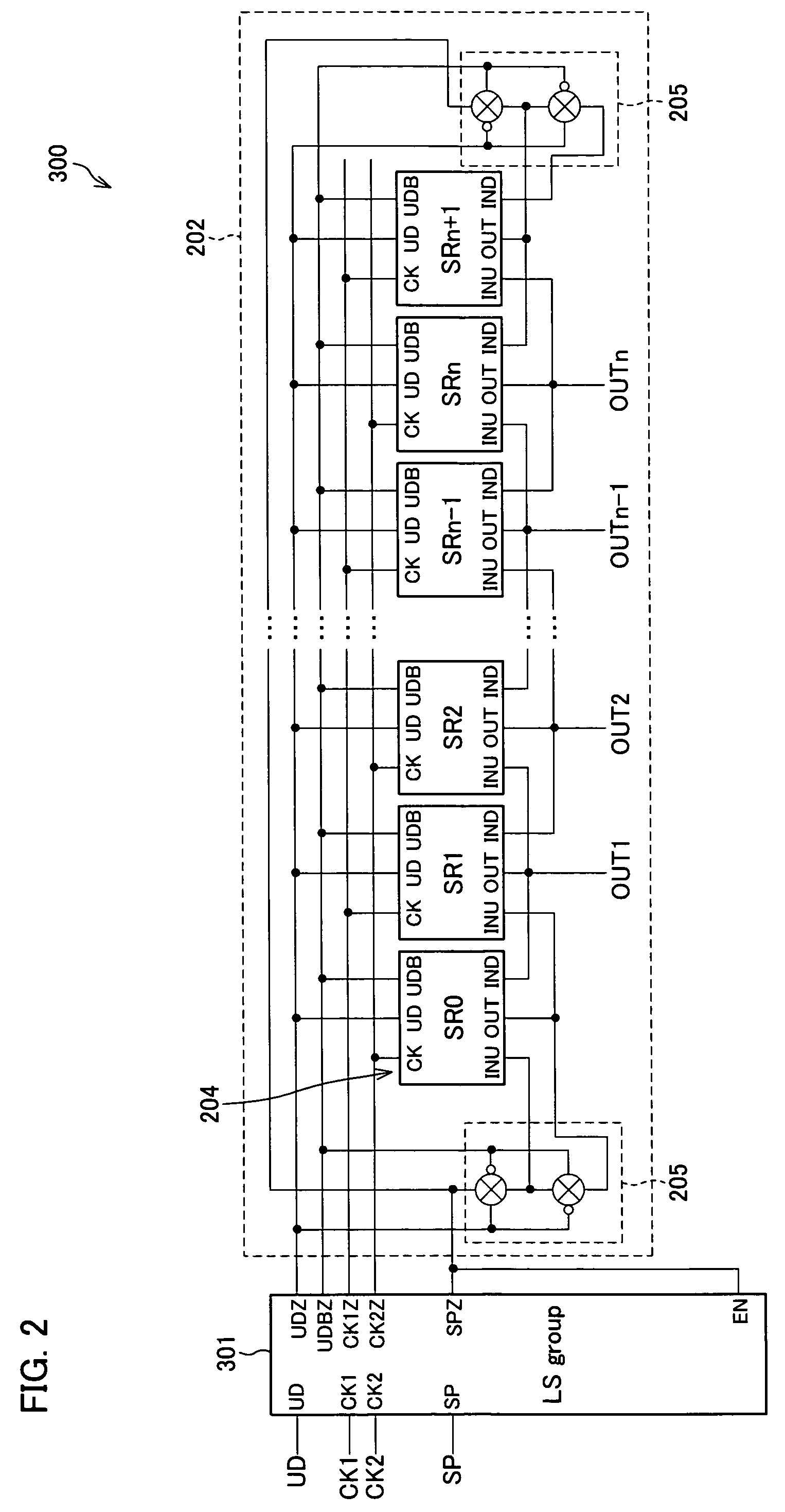
[0051]First, a comparative example of the present invention will be discussed with reference to FIGS. 5–8. FIG. 5 is a block diagram of a scanning signal line drive circuit 200 of the comparative example. In this scanning signal line drive circuit, a level shifter 201a (cf. FIG. 7) steps up a shifting direction switching signal UD (cf. FIG. 6) for switching the shifting direction of the bi-directional shift register, and a stationary current of the level shifter 201a is caused to flow only during a period in which the output on the last stage of the bi-directional shift register 204 (cf. FIG. 5) is HIGH, so that the reduction of the power consumption is realized.

[0052]The scanning signal line drive circuit 200 is manufactured in a monolithic fashion and is made up of a level shifter group 201, a shift register block 202, and a last-stage output selecting circuit 203.

[0053]The level shifter group 201 is made up of level shifters for level-shifting various low-voltage input signals, w...


PUM

PropertyMeasurementUnit
strain pointaaaaaaaaaa
drive voltageaaaaaaaaaa

Abstract

A level-shifter is combined with a bi-directional shift register. The level shifter turns a start signal of the bi-directional shift register to be an enable signal, and (i) activates a level shifting section by supplying a stationary current, during a period in which the enable signal is HIGH, while (ii) deactivates the level shifting section by cutting off the stationary current, during a period in which the enable signal EN is LOW. With this, it is possible to reduce unnecessary current consumption by a level shifter provided for a signal which does not frequently change, such as a shifting direction switching signal for which the bi-directional shift register is provided. At the same time, when such a signal changes, the change is followed with no time lag.

Description

[0001]This Nonprovisional application claims priority under 35 U.S.C. § 119(a) on Patent Application No. 2003 / 328614 filed in Japan on Sep. 19, 2003, the entire contents of which are hereby incorporated by reference.FIELD OF THE INVENTION[0002]The present invention relates to a level shifter suitably used for a scanning signal line drive circuit and a data signal line drive circuit of a matrix display device, and particularly to the level shifter and a scanning signal line drive circuit, a data signal line drive circuit, and a display device which adopt the level shifter.BACKGROUND OF THE INVENTION[0003]In a scanning signal line drive circuit and a data signal line drive circuit of a matrix display device, shift registers are widely adopted to generate a scanning signal supplied to scanning signal lines and to control the timings for sampling voltages, which are supplied to respective data signal lines, from a video signal.[0004]Meanwhile, being typified by a monitor panel of a vide...

Claims


Application Information

Patent Timeline
Patent Type & Authority Patents(United States)
IPC IPC(8): G09G5/00G09G3/10G02F1/133G09G3/20G09G3/36G11C19/00H03K5/003H03K19/0185
CPCG09G3/20G09G2300/0408G09G2310/0289G09G2310/0275G09G2310/0267G09G3/36G11C19/00
Inventor TSUJINO, SACHIORIKU, HOH
Owner SHARP KK
Why Eureka
Try Eureka