
Imaging system using solid-state CMOS imaging device

a solid-state cmos imaging and imaging system technology, applied in the direction of television systems, radiation controlled devices, color signal processing circuits, etc., can solve the problems of difficult to distinguish light and dark spots produced in the frame from the contents of the picture, the picture quality is remarkably deteriorated, and the power consumption of the image is increased

Inactive Publication Date: 2007-04-24
RENESAS ELECTRONICS CORP
View PDF8 Cites 15 Cited by
  • Summary
  • Abstract
  • Description
  • Claims
  • Application Information

AI Technical Summary

Benefits of technology

[0015]It is a first object of the present invention to provide flicker canceling technique capable of preventing light and dark spots appearing in a picture frame due to flicker of an illumination light source such as a fluorescent lamp in an imaging system such as a video camera using a solid-state CMOS imaging device effectively by means of relatively simple constituent means.
[0016]It is a second object of the present invention to provide technique capable of performing automatic iris adjustment widely and smoothly while preventing reduction of picture quality due to flicker of a light source effectively in an imaging system using a solid-state CMOS imaging device.
[0017]It is a third object of the present invention to provide technique capable of automatically judging whether flicker due to a fluorescent lamp is produced or not prior to canceling of the flicker in an imaging system using a solid-state CMOS imaging device without provision of dedicated measures such as a photodiode.
[0018]According to a first aspect of the present invention, an imaging system using a solid-state CMOS imaging device, comprising charge storage control means for setting up an electric charge storage time for each pixel to be equal to a turning-on-and-off period of a fluorescent lamp or an integral multiple thereof. Thus, flicker due to an illumination light source such as the fluorescent lamp appearing as light and dark spots in a frame can be prevented effectively by means of simple constituent means.
[0020]Further, in the above aspect, when the charge storage time is set up while using a horizontal scanning line as a unit, the function of the solid-state CMOS imaging device is utilized to make it possible to set up the charge storage time simply and exactly. Further, the charge storage time is changed over in response to the turning-on-and-off period of the light source illuminating the object to be imaged or the integral multiple thereof to set up the stored light amount for each pixel variably stepwise and difference in the stored light amounts between steps is interpolated by means of continuous gain control of read-out signals of pixels, so that automatic iris adjustment can be made widely and smoothly while preventing flicker due to an illumination light source such as a fluorescent lamp effectively. In this case, the gain control can be performed in any one or both of the inside and the outside of the solid-state CMOS imaging device.
[0024]Further, only detection circuits for the small-area brightness and the large-area brightness are provided in a semiconductor integrated circuit for processing read-out signals of pixels and brightness levels detected by the detection circuits are sent to a microcomputer so that judgment as to whether flicker is produced or not on the basis of the brightness levels is performed by means of processing in accordance with a software of the microcomputer to thereby make it possible to suppress an increased circuit scale of the semiconductor integrated circuit for processing the read-out signals of the pixels and reduce a chip size.

Problems solved by technology

Consequently, the power consumption thereof is increased.
However, in a camera system using the solid-state CMOS imaging device, as shown in FIG. 5, it is ascertained that influence due to the flicker of the fluorescent lamp appears as light and dark spots in a striped pattern and the picture quality is deteriorated remarkably.
The light and dark spots produced in the frame are difficult to distinguish from contents of a picture and cannot be corrected by a conventional technique such as AGC.

Method used


Image

  • Imaging system using solid-state CMOS imaging device
  • Imaging system using solid-state CMOS imaging device
  • Imaging system using solid-state CMOS imaging device

Examples


first embodiment

(First Embodiment)

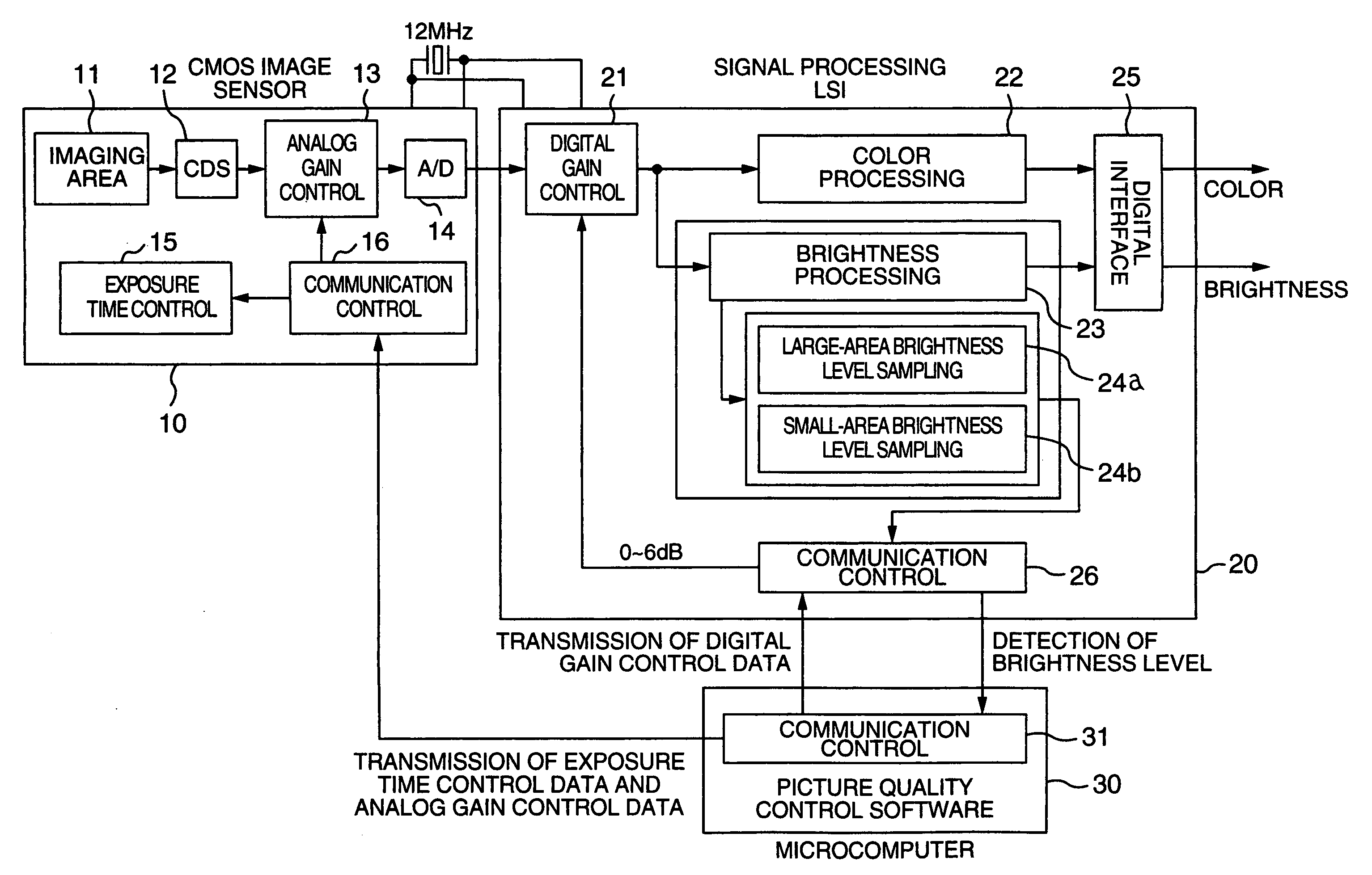
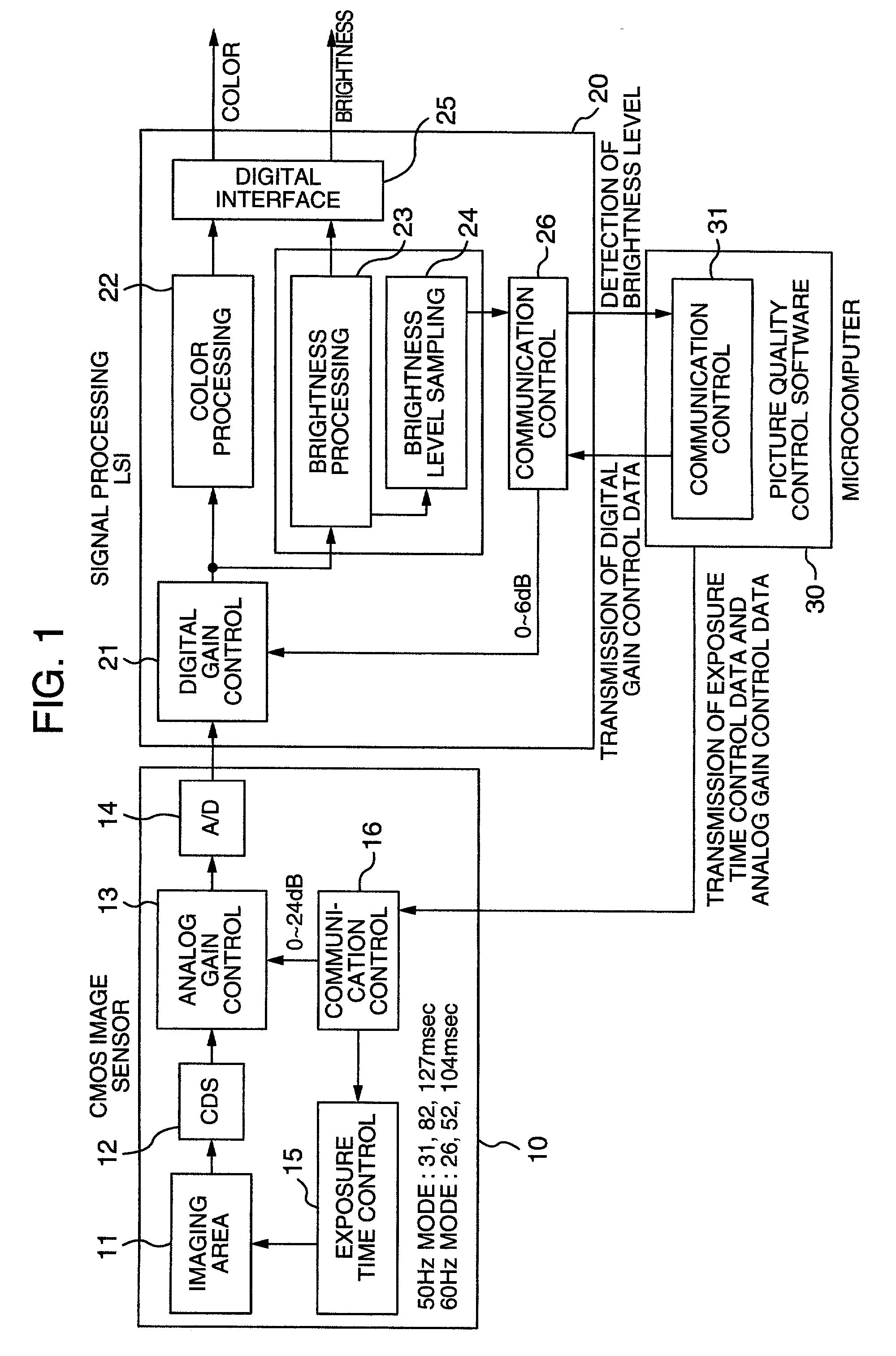
[0040]FIG. 1 is a block diagram schematically illustrating a first embodiment of a camera system using a solid-state CMOS imaging device to which the technique of the present invention is applied. The camera system shown in FIG. 1 includes a solid-state CMOS imaging device (image sensor) 10, a signal processing LSI 20 and a system controller 30 constituted by a single-chip microcomputer or the like.

[0041]The solid-state CMOS imaging device 10 includes an imaging area 11, a CDS circuit 12, an analog type gain control circuit 13, an A-D converter 14, a charge storage time control circuit 15 and a communication control unit 16, which are integrated on the same semiconductor substrate.

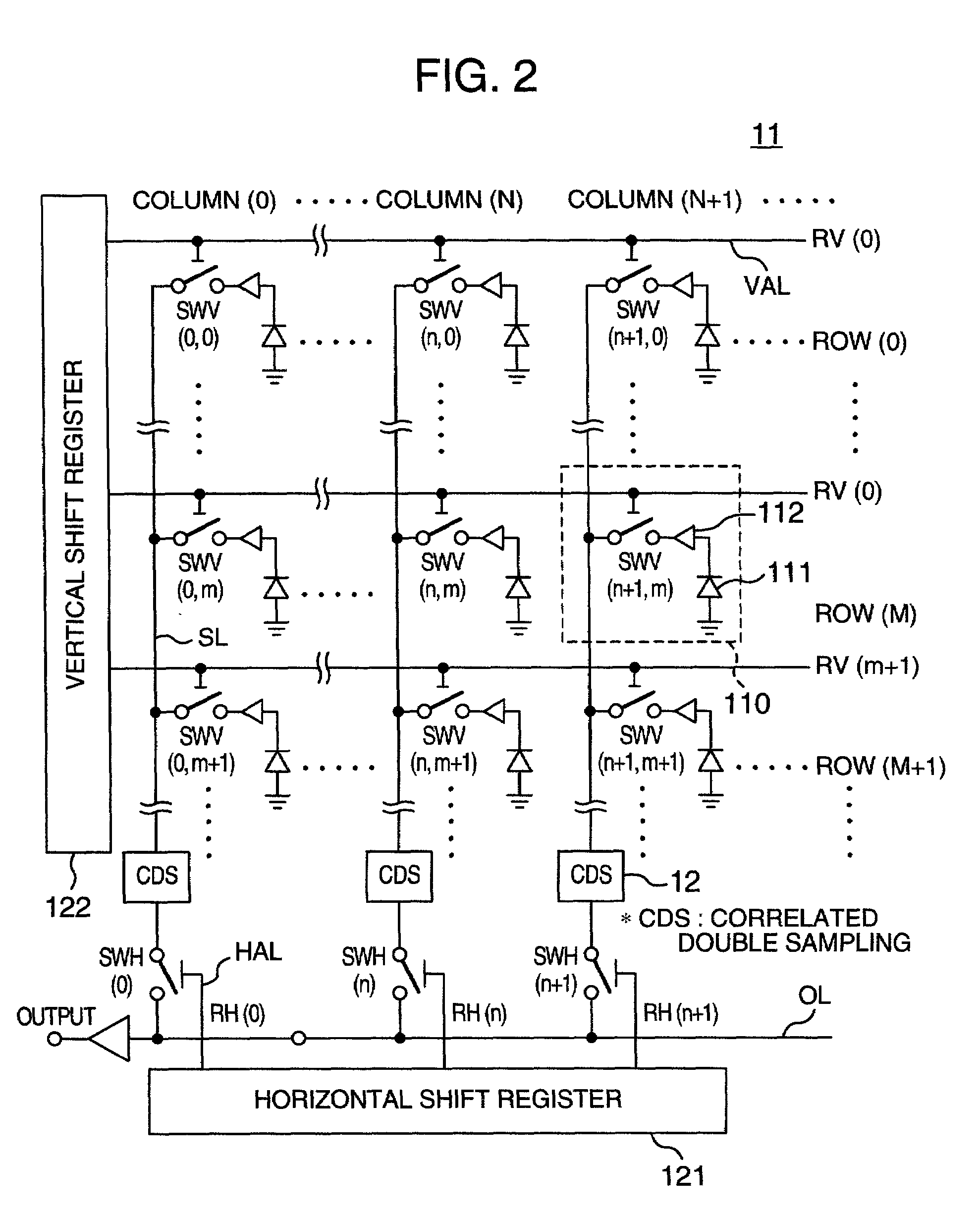
[0042]As shown in FIG. 2, the imaging area 11 is formed of a large number of unit cells or pixels 110 arranged into a matrix having rows (horizontal) and columns (vertical). Each pixel 110 is composed of a photodiode 111, an amplifier 112 and a selection switch SWV and is selected one by ...

second embodiment

(Second Embodiment)

[0060]FIG. 11 is a block diagram schematically illustrating a second embodiment of a camera system using a solid-state CMOS imaging device to which the technique of the present invention is applied. The camera system shown in FIG. 11 includes, similarly to the first embodiment, the solid-state CMOS imaging device (image sensor) 10, the signal processing LSI 20 and the system controller 30, which can be mounted on a printed wiring board, for example, to be constituted as a module.

[0061]In this case, a lens can be mounted on a package of the solid-state CMOS imaging device 10 in corresponding manner to an imaging area to constitute a module. With constitution of the module, it is easy to incorporate the imaging function into a portable data terminal and a portable telephone such as a PDA (Personal Digital Assistants) and the apparatus can be constituted to be compact. Further, the signal processing circuit 20 and the system controller (single-chip microcomputer) 30 ...


PUM


Abstract

Turning on and off of the light source illuminating an object to be imaged is judged based on brightness changes in small and large areas set up in the frame and an electric charge storage time for each pixel is set up to be equal to the turning-on-and-off period of the light source or an integral multiple thereof. The charge storage time is changed over responsive to the turning-on-and-off period of the light source or the integral multiple thereof to set up a stored light amount for each pixel stepwise and difference in the stored light amount between steps is interpolated by continuous gain control of read-out signals of pixels.

Description

BACKGROUND OF THE INVENTION[0001]The present invention relates to effective technique applied to an imaging system using a solid-state CMOS imaging device and more particularly to effective technique utilized to cancel flicker of a fluorescent lamp in a camera system including automatic iris adjustment function for controlling brightness of an imaged picture in accordance with photographic surroundings.[0002]As an imaging device for a video camera or an electronic still camera, there are a solid-state CCD imaging device and a solid-state CMOS imaging device. The solid-state CMOS imaging device has merits that power consumption thereof is smaller as compared with the solid-state CCD imaging device and it is suitable for compactness and lightness in weight of a video camera and a digital camera. In the solid-state CCD imaging device, electric charges photoelectrically converted and stored for each pixel are transferred to a CCD for transfer simultaneously in parallel at the same timin...

Claims


Application Information

Patent Timeline
Patent Type & Authority Patents(United States)
IPC IPC(8): H04N3/14H04N9/73H01L27/146H04N5/21H04N23/76H04N25/00
CPCH04N5/235H04N5/2351H04N5/2353H04N5/2357H04N5/243H04N23/745H04N23/71H04N23/73H04N23/70H04N23/76H04N25/76
Inventor MATSUMOTO, HIROYUKITAKAHASHI, TAKASHIODAKA, TERUAKINAKAMURA, MASASHISHIDA, KOJI
Owner RENESAS ELECTRONICS CORP
Learn More