Circuit substrate and method for fabricating the same

a technology of circuit substrate and substrate, which is applied in the direction of printed circuit manufacturing, printed circuit aspects, printed element electric connection formation, etc., can solve the problems of dielectric breakdown, electrical components often come off, leak current, etc., and achieve the effect of reducing the stress generated in the core substrate, increasing the surface roughness of the inside walls, and reducing the stress of the core substra

a technology of circuit substrate and substrate, which is applied in the direction of printed circuit manufacturing, printed circuit aspects, printed element electric connection formation, etc., can solve the problems of dielectric breakdown, electrical components often come off, leak current, etc., and achieve the effect of reducing the stress generated in the core substrate, increasing the surface roughness of the inside walls, and reducing the stress of the core substra

US7211899B2Inactive Publication Date: 2007-05-01FUJITSU LTD

Image

  • Circuit substrate and method for fabricating the same
  • Circuit substrate and method for fabricating the same
  • Circuit substrate and method for fabricating the same

Examples


first embodiment

[0037][A First Embodiment]

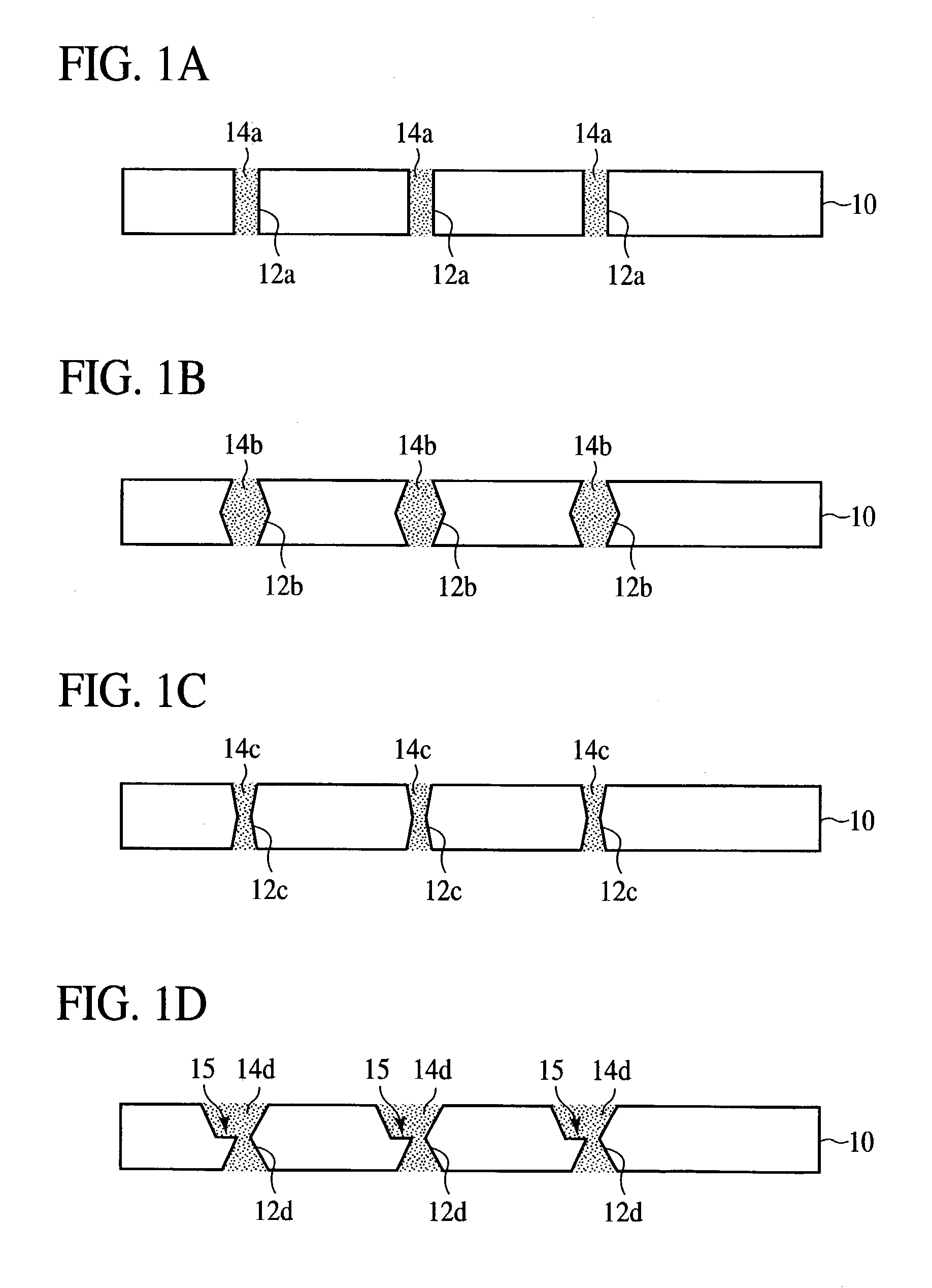
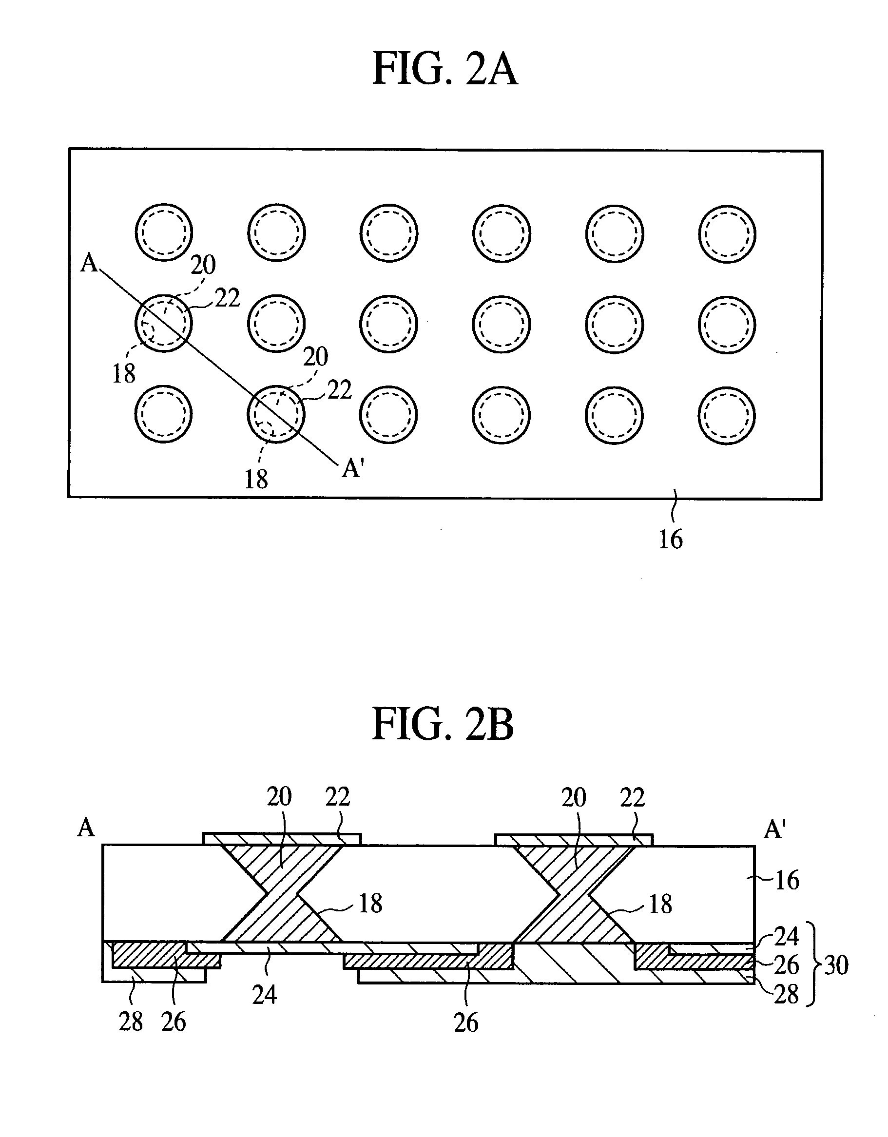
[0038]The circuit substrate according to a first embodiment of the present invention will be explained with reference to FIGS. 2A, 2B, 3A, 3B, 3C, 3D, 4A, 4B, and 4C. FIGS. 2A and 2B are diagrammatic views of the circuit substrate according to the present embodiment, which show a structure thereof. FIGS. 3A, 3B, 3C, 3D, 4A, 4B, and 4C are sectional views of the circuit substrate according to the present embodiment in the steps of the method for fabricating the circuit substrate, which show the method.

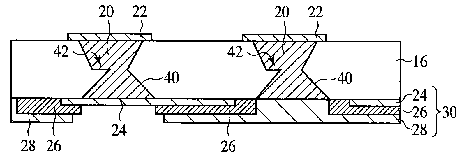
[0039]First, the structure of the circuit substrate according to the present embodiment will be explained with reference to FIGS. 2A and 2B. FIG. 2A is a top view of the circuit substrate according to the present embodiment. FIG. 2B is a sectional view along the line A–A′ in FIG. 2A.

[0040]As shown in FIGS. 2A and 2B, through-holes 18 are formed in a 500 μm-thickness glass substrate 16 at a prescribed pitch. A shape of the through-holes 18 as viewed perpendicula...


PUM

PropertyMeasurementUnit
thicknessaaaaaaaaaa
widthaaaaaaaaaa
thicknessaaaaaaaaaa

Abstract

A circuit substrate comprises a glass substrate 16, through-holes 18 formed through the glass substrate 16 and via electrodes 20 buried in the through-holes 18. An opening width of the through-holes 18 is minimum inside the glass substrate and is increased toward both surfaces of the glass substrate 16. Accordingly, the detachment of the via electrodes 20 can be prevented without increasing the surface roughness of the inside walls of the through holes, and stresses generated in the core substrate can be mitigated.

Description

CROSS-REFERENCE TO RELATED APPLICATION[0001]This application is based upon and claims priority of Japanese Patent Application No. 2002-9442, filed on Jan. 18, 2002, the contents being incorporated herein by reference.BACKGROUND OF THE INVENTION[0002]The present invention relates to a circuit substrate and a method for fabricating the circuit substrate which are adaptable to higher density and higher speed.[0003]Recently, semiconductor parts used in computers, etc. are rapidly made increasingly adaptable to higher density and higher speed. Circuit substrates as well are accordingly required to be adaptable to the higher density and the higher speed.[0004]One example of the conventional circuit substrates will be explained with reference to FIGS. 9A and 9B. FIG. 9A is a sectional view of the mounted conventional circuit substrate, which shows the structure of the circuit substrate. FIG. 9B is a perspective view of the circuit substrate, which shows the structure of the circuit substra...

Claims


Application Information

Patent Timeline
01 May 2007
Publication
US7211899B2
IPC
H01L23/48; H01L23/15; H05K3/46; H01L23/498; H05K1/03; H05K1/11; H05K3/00
CPC
H01L23/481; H01L23/49827; H05K1/115; H05K3/0044; H01L23/15; H01L2224/16; H01L2924/01046; H01L2924/01077
Inventors
TANIGUCHI, OSAMU; YAMAGISHI, YASUO