Spin-orbital quantum cellular automata logic devices and systems

a quantum cell and logic device technology, applied in the field of nanocomputing, can solve the problems of inability to reduce critical dimensions further, lack of logic architecture which would ensure input isolation, and higher decoherence ra

Inactive Publication Date: 2007-05-01
INTEL CORP
View PDF3 Cites 13 Cited by
  • Summary
  • Abstract
  • Description
  • Claims
  • Application Information

AI Technical Summary

Problems solved by technology

However, as critical device dimensions approach atomic length scales, it will not be possible to reduce critical dimensions further, and alternative means of storing and manipulating information must be found.
The disadvantages of this computing paradigm include a basic trade off between the tight coupling between spins and the resulting higher decoherence rate as well as a lack of logic architecture which would ensure input isolation.
This approach suffers from several problems including sensitivity to stray charge, system hang up in metastable states, asynchronous operation and others.

Method used


Image

  • Spin-orbital quantum cellular automata logic devices and systems
  • Spin-orbital quantum cellular automata logic devices and systems
  • Spin-orbital quantum cellular automata logic devices and systems

Examples


Embodiment Construction

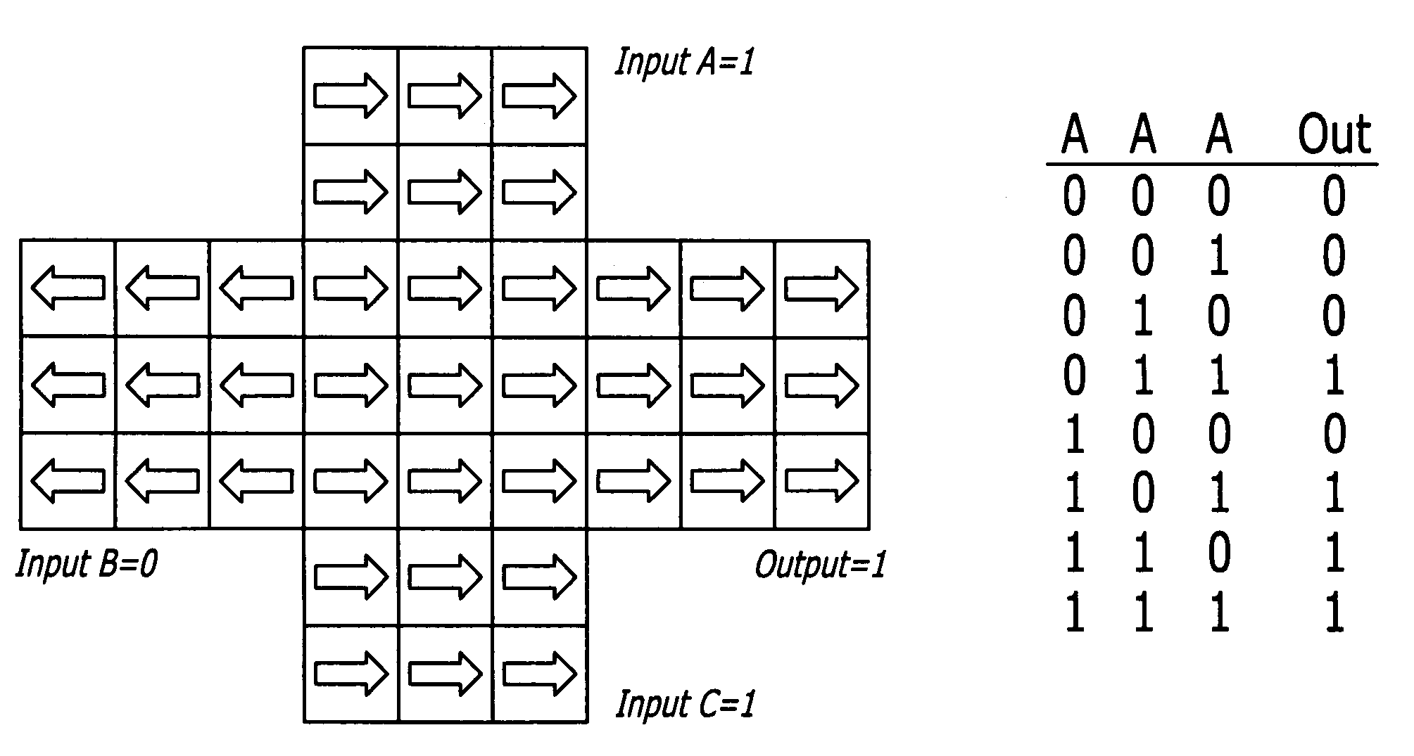
[0017]Embodiments of the present invention may be differentiated from prior art in that it enables continuous scaling of the size of the unit cells intrinsic to QCA down to the atomic sizes and the physical attributes that stores the information (coupled ferromagnetic and transport phase states).

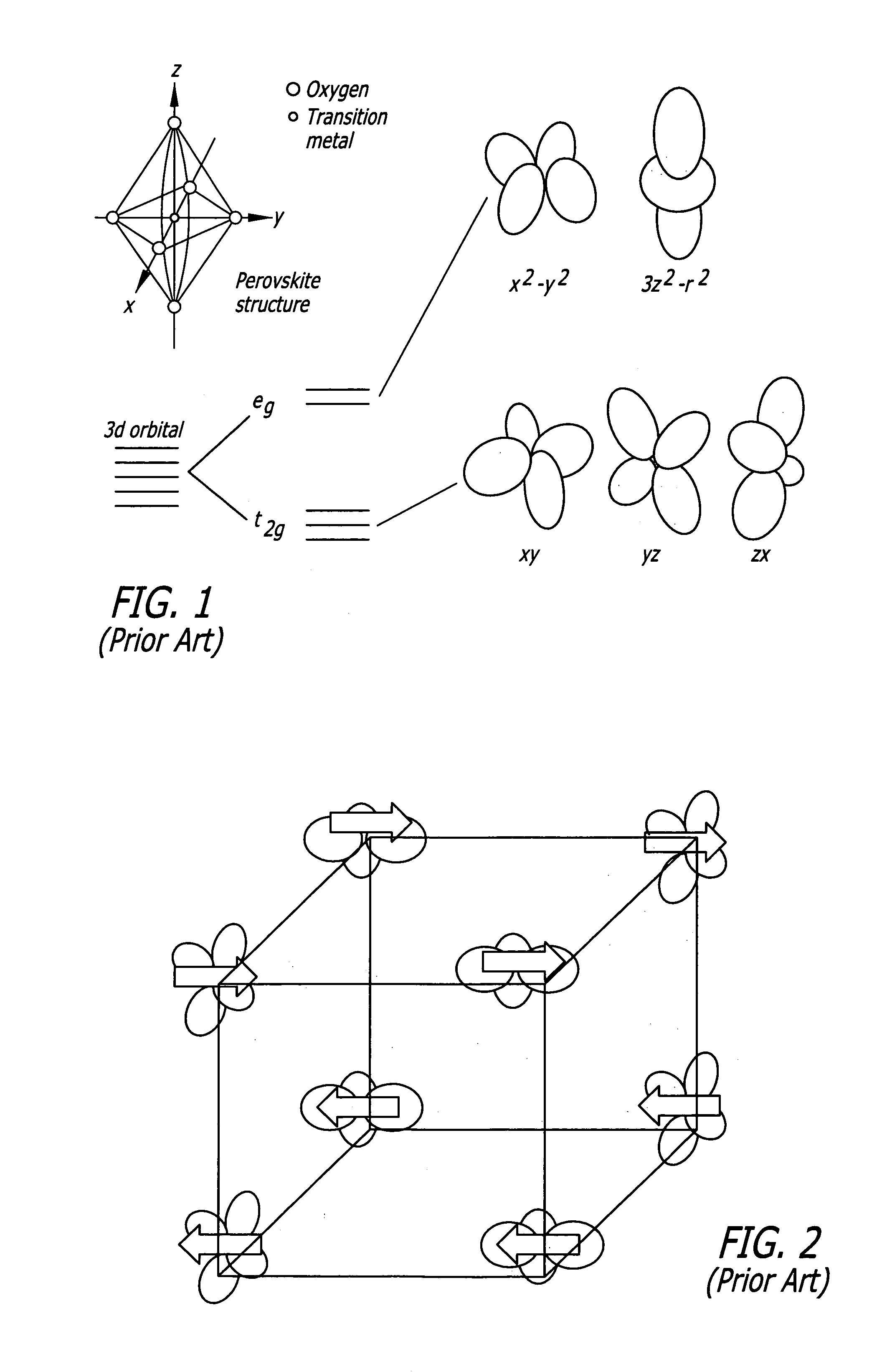
[0018]The embodiments use a novel implementation of the quantum cellular automata (QCA) architecture QCA systems that use unit cells physically configured so they spontaneously interact with each other in a sequential fashion to perform logic operations. In particular, certain crystalline materials, such as transition metal oxides, exhibit strongly correlated electronic, structural and magnetic effects. The manganese atoms in certain manganite crystals have an energy band structure as shown in FIG. 1, where the energy levels are associated with different orbital states of the 3d shell electrons. In the Figure, the electron wavefunction amplitudes are illustrated by the smooth shaded objects ...


PUM


Abstract

Spin-orbital quantum cellular automata logic devices and integrated circuits in the form of a substrate having a thin film of material on the substrate having strongly coupled spin-orbital states, the thin film being patterned to define at least one input and at least one output, and to perform at least one logic operation by associated arrangement of the spin-orbital states between the input and the output. The logic devices and integrated circuits further include an input device at each input to define the spin-orbital states at each input, and an output sensor at each output for sensing the spin-orbital states of the thin film at the output. In an integrated circuit, the output of one gate or circuit, in the form of the ferromagnetically aligned spins, can be directly coupled to the next gate or circuit, so that entire circuits can be fabricated and effectively interconnected, only requiring interfacing for overall. circuit input and output using the electromagnetic inputs and magnetic measurements for the outputs.

Description

BACKGROUND OF THE INVENTION[0001]1. Field of the Invention[0002]The embodiments of the present invention relate to the field of nanocomputing.[0003]2. Prior Art[0004]Embodiments of the present invention are intended to produce logic devices that are smaller, faster, less expensive, and more power efficient than anticipated 16 nm CMOS devices. Presently such goals are pursued by dimensional scaling (reducing gate length, operating voltage) and have improved transistor performance for multiple generations. However, as critical device dimensions approach atomic length scales, it will not be possible to reduce critical dimensions further, and alternative means of storing and manipulating information must be found.[0005]Conventional computing devices including CMOS devices associate computational state (information) with electronic charge and then manipulate, store and detect those charges to perform logic operations. However, computational state can be associated with other physically c...

Claims


Application Information

Patent Timeline
Patent Type & Authority Patents(United States)
IPC IPC(8): H03K19/195
CPCH03K19/02H03K19/16
Inventor BOURIANOFF, GEORGE I.NIKONOV, DMITRI E.ZHENG, JUN-FEI
Owner INTEL CORP
Why Eureka
Try Eureka